
300mm SiC Wafer Processing After the 12-Inch Breakthrough: Slicing, Grinding, CMP, Edge Exclusion and Yield Challenges
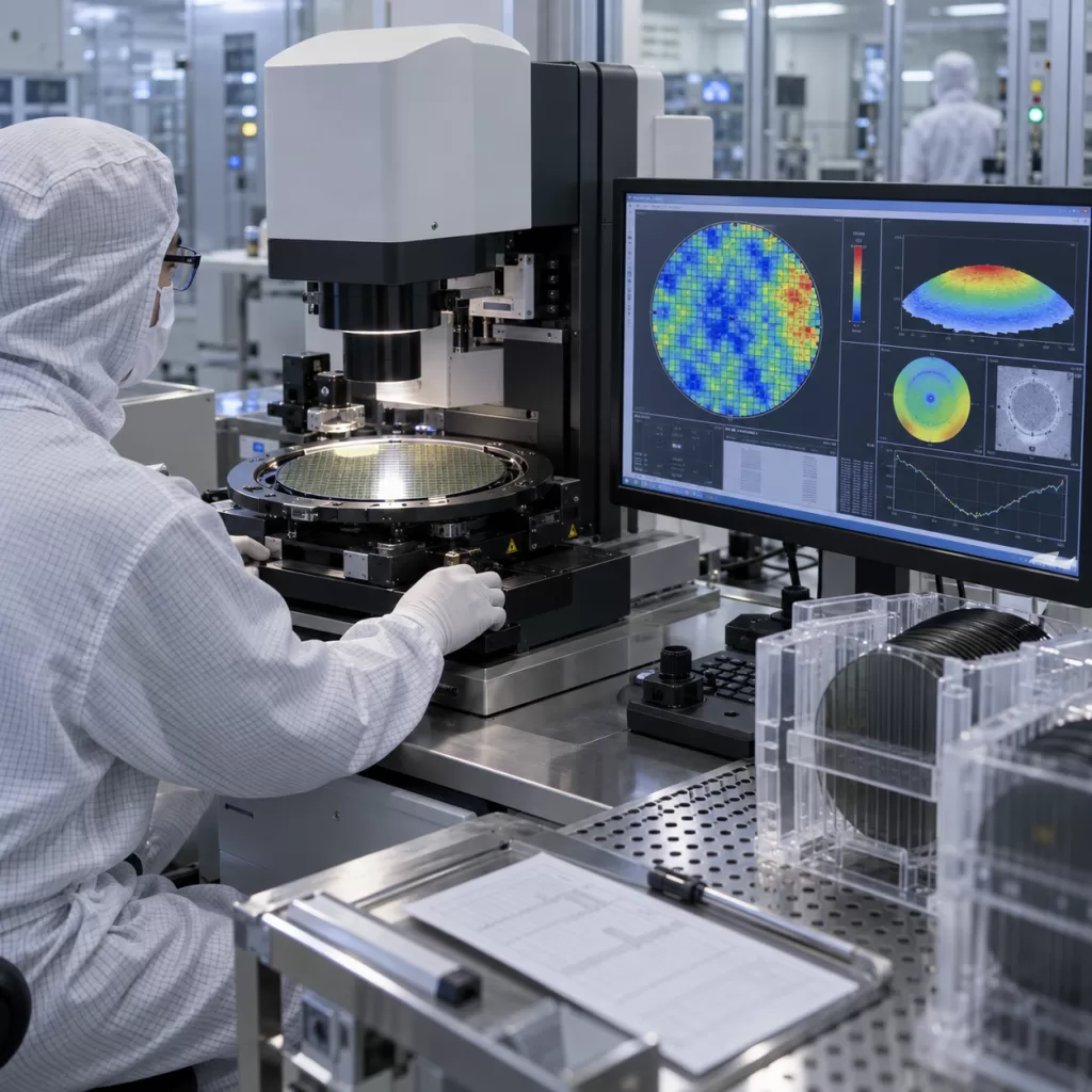
The transition of silicon carbide wafers from 150 mm to 200 mm has already forced the SiC industry to rethink crystal growth, wafer flatness, defect control and equipment compatibility. The emergence of 300 mm, or 12-inch, SiC substrates raises those challenges to an entirely different level. In September 2026, Resonac reported that it had successfully […]
How to Qualify an 8-Inch SiC Wafer Supplier in 2026: Defect Maps, TTV, Bow, Warp, Epi Quality, CoA and Lot Traceability
The transition from 150 mm to 200 mm (8-inch) silicon carbide wafers is changing how semiconductor manufacturers evaluate SiC substrate suppliers. At 150 mm, a buyer may sometimes begin qualification with basic parameters such as diameter, thickness, resistivity, surface roughness and micropipe density. For 200 mm production, that is no longer enough. As wafer diameter […]
300mm High-Thermal-Conductivity SiC Substrates for AI/HPC Packaging: Thermal Conductivity, Flatness, Thickness and Bonding Requirements

Artificial intelligence accelerators and high-performance computing processors are creating a thermal-management problem that can no longer be solved only by improving external heat sinks or cooling systems. As GPU, accelerator, HBM and chiplet integration becomes denser, a growing portion of the thermal challenge is moving inside the semiconductor package itself. The material directly beneath or […]
2026 Marks a Turning Point for Silicon Carbide: From “Who Can Make It?” to “Who Can Make It Cheaper?”
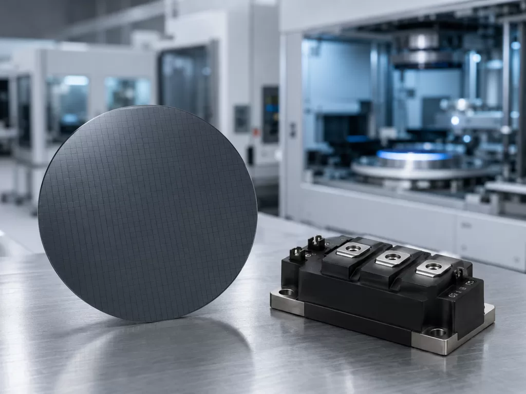
For years, the silicon carbide industry had one overriding question: Who can manufacture high-quality SiC at scale? Crystal growth was difficult. Wafer supply was limited. Defect control was challenging. Device capacity was insufficient, and demand from electric vehicles encouraged manufacturers throughout the supply chain to expand aggressively. In 2026, however, the competitive landscape is changing. […]
300mm vs. 200mm SiC Wafer Cost Analysis: At What Production Volume is the 12-Inch Transition Profitable?
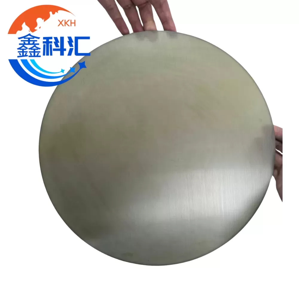
Silicon carbide (SiC) wafers have become a critical material for high-power electronics, electric vehicles, and advanced semiconductor devices. As the demand for higher efficiency, smaller form-factor devices grows, semiconductor manufacturers face a strategic decision: whether to transition from conventional 200mm (8-inch) SiC wafers to 300mm (12-inch) wafers. While larger wafers promise cost savings per device, […]
300mm SiC Wafers Challenges: The Technical Hurdles of Crystal Growth in Larger Diameters (EFG vs. PVT)
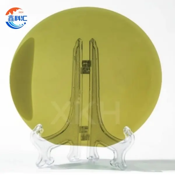
Silicon carbide (SiC) has emerged as a cornerstone material for high-power electronics, electric vehicles, and next-generation semiconductor devices due to its exceptional thermal conductivity, high breakdown voltage, and chemical stability. As the semiconductor industry pushes for larger wafer diameters to reduce production costs and increase throughput, the transition from conventional 150mm and 200mm SiC wafers […]
300 mm Silicon Carbide Wafers: Materials, Manufacturing Barriers, and the Path to Industrial-Scale Wide-Bandgap Semiconductors
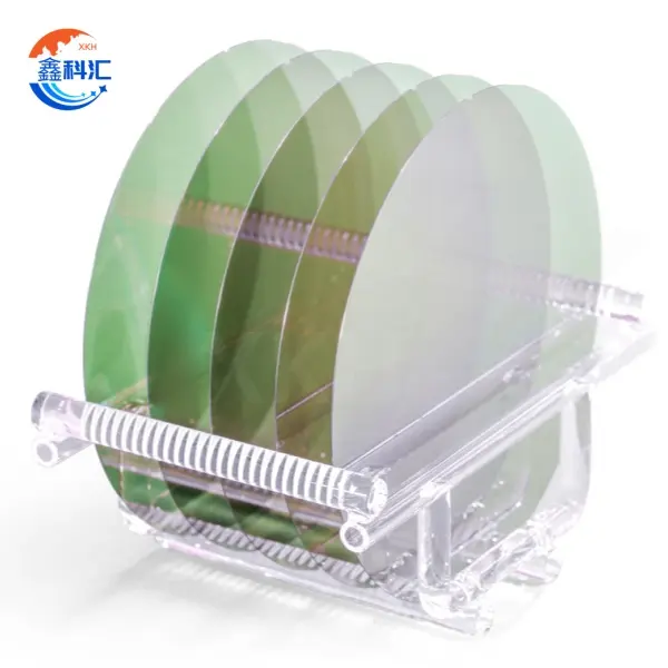
1. Introduction: From Wafer Diameter to Industrial Capability In semiconductor technology, wafer diameter has historically served as a reliable indicator of manufacturing maturity. Each major transition in wafer size—from 150 mm to 200 mm, and later to 300 mm—has marked a shift from laboratory-scale innovation to industrial-scale production. These transitions are not merely geometric expansions; […]