
Laser Stealth Dicing of SiC Wafers: Subsurface Microcracks, Edge Chipping, Dicing Quality, Inspection and Yield Control
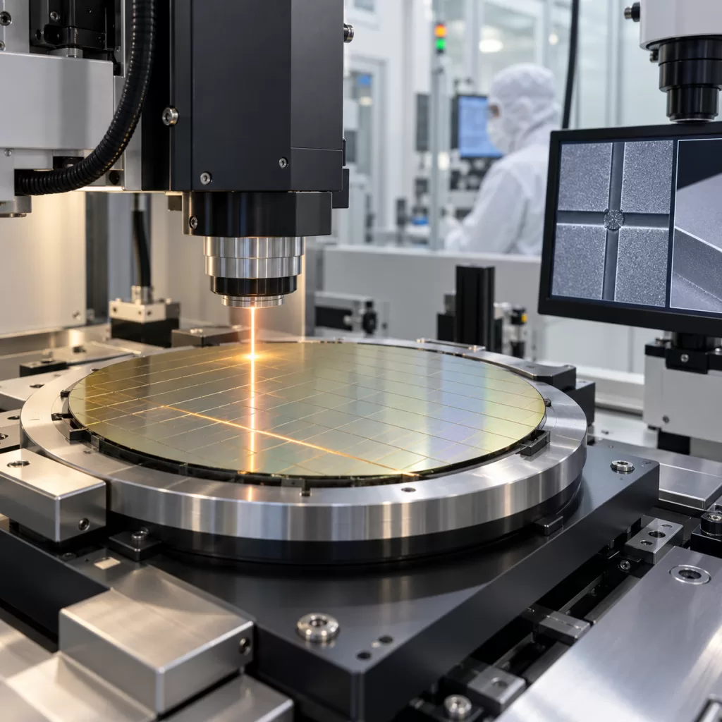
Silicon carbide wafers are increasingly used in high-power and high-temperature semiconductor devices, but they also present major challenges during singulation. Because SiC is extremely hard and brittle, conventional blade dicing can cause edge chipping, kerf loss, mechanical stress and tool wear. As device structures become smaller and wafer value increases, manufacturers are paying more attention […]
300mm SiC Wafer Processing After the 12-Inch Breakthrough: Slicing, Grinding, CMP, Edge Exclusion and Yield Challenges
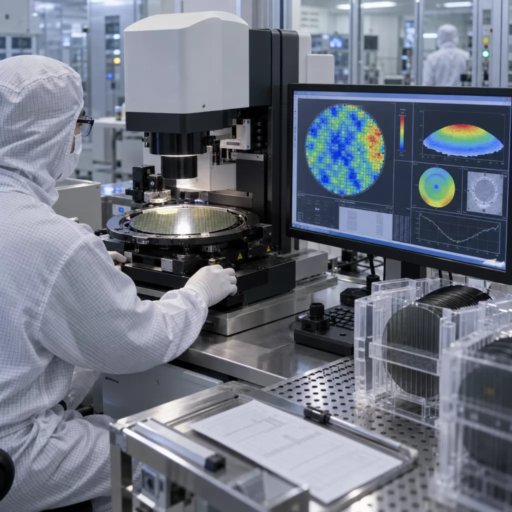
The transition of silicon carbide wafers from 150 mm to 200 mm has already forced the SiC industry to rethink crystal growth, wafer flatness, defect control and equipment compatibility. The emergence of 300 mm, or 12-inch, SiC substrates raises those challenges to an entirely different level. In September 2026, Resonac reported that it had successfully […]
How to Qualify an 8-Inch SiC Wafer Supplier in 2026: Defect Maps, TTV, Bow, Warp, Epi Quality, CoA and Lot Traceability
The transition from 150 mm to 200 mm (8-inch) silicon carbide wafers is changing how semiconductor manufacturers evaluate SiC substrate suppliers. At 150 mm, a buyer may sometimes begin qualification with basic parameters such as diameter, thickness, resistivity, surface roughness and micropipe density. For 200 mm production, that is no longer enough. As wafer diameter […]
8-Inch SiC Wafer Specifications: Diameter, Thickness, Resistivity and Defect Limits
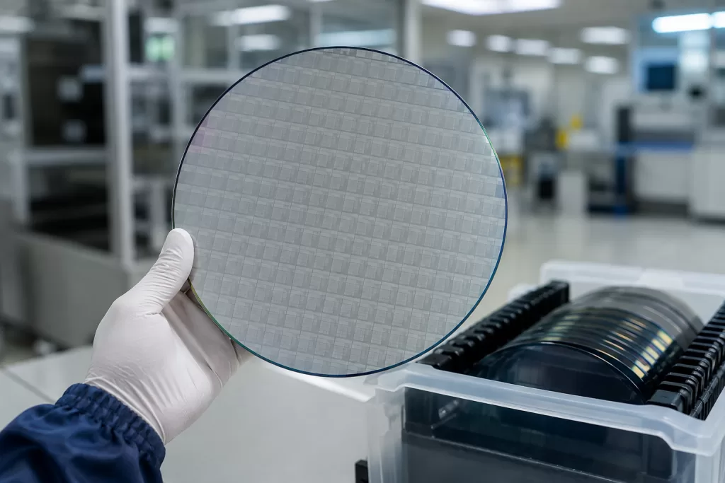
Silicon carbide (SiC) has become one of the most important semiconductor materials for high-power, high-voltage and high-frequency applications. As electric vehicles, renewable energy systems, AI power supplies and industrial automation continue to grow, the demand for larger SiC substrates is increasing rapidly. Compared with traditional 6-inch wafers, 8-inch (200 mm) SiC wafers provide more usable […]