
Silicon Carbide (SiC) has emerged as one of the most important semiconductor materials for next-generation power electronics. Thanks to its wide bandgap, high thermal conductivity, and superior breakdown electric field, SiC devices offer significant advantages over traditional silicon-based technologies in electric vehicles, renewable energy systems, industrial drives, and high-voltage power conversion.
Despite these advantages, manufacturing high-quality SiC wafer remains one of the most technically demanding processes in the semiconductor industry. Compared with silicon wafers, SiC substrates are more difficult to grow, process, and polish due to their unique material properties.
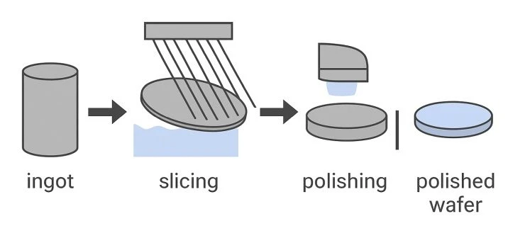
From crystal growth to wafer slicing and chemical mechanical polishing (CMP), every stage presents significant engineering challenges that directly affect wafer quality, yield, and cost.
This article explores the major difficulties encountered in SiC wafer manufacturing and explains why producing defect-free SiC substrates remains a critical industry challenge.
Why Is SiC More Difficult to Manufacture Than Silicon?
The primary reason lies in the physical properties of silicon carbide.
Compared with silicon, SiC exhibits:
| Property | Silicon (Si) | Silicon Carbide (4H-SiC) |
|---|---|---|
| Bandgap | 1.12 eV | 3.26 eV |
| Mohs Hardness | 7 | 9.2–9.5 |
| Thermal Conductivity | ~150 W/m·K | ~490 W/m·K |
| Sublimation Temperature | 1414°C (melting) | >2700°C |
| Chemical Stability | Moderate | Extremely High |
These properties make SiC an outstanding semiconductor material, but they also make it exceptionally difficult to process.
1. Crystal Growth Challenges
Physical Vapor Transport (PVT) Growth
Most commercial SiC boules are produced using the Physical Vapor Transport (PVT) method.
In this process:
- High-purity SiC powder is heated above 2000°C.
- The material sublimates into vapor species.
- Vapor condenses onto a seed crystal.
- A single crystal gradually grows over several days.
Unlike silicon, SiC cannot be grown using conventional melt-growth techniques because it decomposes before melting.
Extreme Temperature Control
One of the biggest challenges is maintaining precise thermal conditions.
Typical growth temperatures range from:
- 2000°C to 2400°C
Even slight temperature fluctuations can lead to:
- Polytype instability
- Crystal stress
- Defect generation
- Reduced crystal quality
Maintaining a stable thermal gradient throughout the growth chamber is critical.
Crystal Defect Formation
SiC crystals are susceptible to various defects, including:
Micropipes
Hollow-core screw dislocations that can significantly reduce device yield.
Threading Screw Dislocations (TSD)
Defects that increase leakage current and lower breakdown voltage.
Threading Edge Dislocations (TED)
Common defects that affect carrier transport.
Basal Plane Dislocations (BPD)
A major reliability concern for bipolar power devices.
Reducing defect density remains one of the industry’s most important objectives.
Scaling from 6-Inch to 8-Inch Wafers
As demand for SiC power devices grows, manufacturers are transitioning from:
- 150 mm (6-inch)
- to 200 mm (8-inch)
However, larger crystal diameters introduce additional challenges:
- Thermal stress accumulation
- Crystal cracking
- Defect propagation
- Growth uniformity control
Maintaining crystal quality across larger wafers requires advanced furnace design and process optimization.
2. SiC Wafer Slicing Challenges
Exceptional Material Hardness
SiC is one of the hardest semiconductor materials available.
Its hardness approaches that of sapphire and is second only to diamond among commonly used semiconductor substrates.
Consequently:
- Conventional wire sawing is slower.
- Tool wear is severe.
- Cutting costs increase significantly.
Kerf Loss and Material Waste
During slicing, part of the crystal is lost as kerf.
Because SiC boules are expensive to produce, reducing material loss is economically important.
Manufacturers continuously seek to:
- Minimize kerf width
- Improve slicing efficiency
- Increase wafer yield per boule
Surface Damage
Mechanical slicing introduces:
- Micro-cracks
- Residual stress
- Surface roughness
- Subsurface damage
These defects must be removed during subsequent grinding and polishing steps.
Failure to eliminate damaged layers can negatively affect device reliability.
Emerging Laser Slicing Technologies
To improve material utilization, laser-based slicing technologies are gaining attention.
Advantages include:
- Reduced kerf loss
- Higher throughput
- Lower material waste
- Potential cost reduction
Many industry experts view laser slicing as a key technology for future 8-inch SiC wafer production.
3. Grinding and Thinning Challenges
After slicing, wafers must be ground to achieve target thickness.
Typical SiC wafer thicknesses:
| Diameter | Typical Thickness |
| 4 Inch | ~350 μm |
| 6 Inch | ~500 μm |
| 8 Inch | ~500–700 μm |
Grinding challenges include:
- Maintaining TTV control
- Preventing wafer breakage
- Minimizing residual stress
- Achieving uniform thickness
As wafers become thinner, mechanical handling becomes increasingly difficult.
4. Polishing Challenges
Why Polishing Is Difficult
Polishing SiC is significantly harder than polishing silicon.
The reasons include:
- High hardness
- High chemical inertness
- Strong covalent bonding
Traditional polishing methods are often inefficient.
Surface Quality Requirements
Modern epitaxial growth requires atomically smooth surfaces.
Typical specifications include:
- Surface roughness (Ra) < 0.1 nm
- Low defect density
- Minimal subsurface damage
Even nanoscale imperfections can affect epitaxial layer quality.
Chemical Mechanical Polishing (CMP)
CMP is the most widely used finishing process for SiC wafers.
The process combines:
- Chemical surface modification
- Mechanical abrasion
Challenges include:
- Low material removal rate
- High polishing cost
- Slurry optimization
- Surface defect control
Improving CMP efficiency remains a major research area.
Emerging Polishing Technologies
Several advanced polishing techniques are under development:
Plasma-Assisted Polishing
Uses reactive plasma to soften the surface layer.
Catalyst-Referred Etching (CARE)
Provides ultra-smooth surfaces with minimal damage.
Electrochemical Mechanical Polishing (ECMP)
Combines electrochemical reactions with mechanical polishing.
These technologies may significantly improve future wafer quality and productivity.
Cost Implications of Manufacturing Challenges
The complexity of SiC processing contributes directly to wafer cost.
Major cost drivers include:
- Long crystal growth cycles
- High energy consumption
- Low growth yield
- Expensive consumables
- Precision polishing requirements
As manufacturing technologies mature and production scales increase, costs are expected to decline, but SiC wafers will remain substantially more expensive than silicon wafers for the foreseeable future.
Future Industry Trends
Several trends are shaping the future of SiC wafer manufacturing:
Larger Wafer Diameters
Transition toward:
- 200 mm (8-inch) production
Lower Defect Density
Improved crystal growth techniques aim to reduce:
- Micropipes
- BPDs
- TSDs
Advanced Slicing Technologies
Laser slicing and kerf-less approaches are expected to improve material utilization.
High-Efficiency Polishing
New polishing methods seek to achieve:
- Higher throughput
- Better surface quality
- Lower production costs
Conclusion
Manufacturing high-quality SiC wafers is one of the most challenging processes in modern semiconductor production. From crystal growth at temperatures exceeding 2000°C to precision slicing and atomically smooth polishing, every step requires advanced equipment, strict process control, and deep materials expertise.
Although significant progress has been made in recent years, challenges related to crystal defects, wafer scaling, material hardness, and polishing efficiency continue to influence production cost and device performance.
As the demand for electric vehicles, renewable energy systems, and high-power electronics continues to grow, ongoing innovations in crystal growth, slicing, and polishing technologies will play a crucial role in the future expansion of the SiC semiconductor industry.