
1. Introduction: From Silicon Limits to Wide Bandgap Breakthroughs
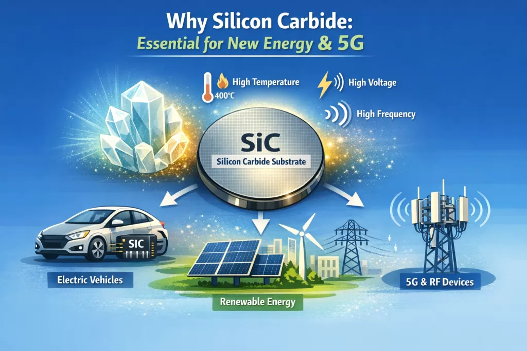
As global industries accelerate toward electrification and digitalization, conventional silicon (Si)-based semiconductors are approaching their physical and performance limits. Applications such as electric vehicles, renewable energy systems, and 5G communications demand devices that can operate under higher voltages, higher temperatures, and higher frequencies.
In this context, silicon carbide (SiC), a representative wide bandgap semiconductor, has emerged as a critical material. Among all SiC-related technologies, the SiC substrate plays a foundational role, serving as the platform upon which high-performance power and RF devices are built. Its material quality directly impacts device efficiency, reliability, and lifetime, making it indispensable in next-generation electronic systems.
2. Fundamental Properties of Silicon Carbide Substrates
Silicon carbide is a compound semiconductor composed of silicon and carbon atoms in a strong covalent lattice. Its intrinsic material properties enable superior performance compared to traditional silicon.
Wide Bandgap (~3.2 eV)
The bandgap of SiC is approximately three times that of silicon, allowing devices to operate at temperatures exceeding 400°C. This reduces the need for complex cooling systems and improves reliability in harsh environments.
High Breakdown Electric Field
SiC exhibits a critical electric field nearly 10 times higher than silicon, enabling devices to handle much higher voltages. This allows for thinner device structures and significantly lower conduction losses.
High Thermal Conductivity
With thermal conductivity about three times greater than silicon, SiC can dissipate heat more efficiently. This is essential for maintaining stable operation in high-power applications.
Low Switching Loss and High Frequency Capability
SiC-based devices offer faster switching speeds and lower energy losses, making them ideal for high-frequency and high-efficiency systems.
These combined properties make SiC substrates uniquely suited for demanding electronic applications where silicon falls short.
3. Manufacturing of SiC Substrates: A High-Barrier Process
The production of silicon carbide substrates is technologically complex and capital-intensive, involving several precision-controlled steps:
1. Single Crystal Growth (PVT Method)
The most widely used technique is Physical Vapor Transport (PVT), where high-purity SiC powder is sublimated at temperatures above 2000°C and recrystallized onto a seed crystal. Precise control of temperature gradients and pressure is critical to minimize defects.
2. Ingot Processing
The grown crystal boule is oriented using X-ray techniques and mechanically shaped into a uniform cylindrical form. This ensures consistent crystal orientation and dimensional accuracy.
3. Wafer Slicing and Surface Preparation
Diamond wire sawing is used to slice the boule into wafers. Subsequent grinding and chemical mechanical polishing (CMP) remove surface damage and produce ultra-smooth, mirror-like surfaces required for epitaxial growth.
4. Cleaning and Inspection
Advanced cleaning processes remove contaminants, while inspection techniques evaluate defects, flatness, and material purity. Only wafers meeting strict standards proceed to device fabrication.
Due to the extreme process conditions and stringent quality requirements, SiC substrate manufacturing remains one of the most technically challenging segments in the semiconductor industry.
4. Core Application Drivers: Why SiC Substrates Are Essential
4.1 Electric Vehicles (EVs)
SiC substrates are widely used in power electronics systems such as inverters, onboard chargers (OBC), and DC-DC converters. Their advantages include:
- Higher energy conversion efficiency
- Reduced power loss and heat generation
- Smaller and lighter system designs
- Extended driving range and faster charging
These benefits make SiC a key enabler for high-performance electric vehicles.
4.2 Renewable Energy and Power Grids
In applications such as photovoltaic inverters, wind power converters, and energy storage systems, SiC devices improve:
- Power conversion efficiency
- System reliability under high loads
- Thermal management performance
They also contribute to reduced energy loss across transmission and distribution networks, supporting global decarbonization goals.
4.3 5G Communication and RF Devices
Semi-insulating SiC substrates are used for GaN-on-SiC RF devices, particularly in 5G base stations. Key advantages include:
- High power density
- उत्कृष्ट heat dissipation
- Stable performance at high frequencies
These characteristics are critical for maintaining signal integrity and efficiency in modern communication infrastructure.
5. Industry Challenges and Future Trends
Despite its advantages, the SiC substrate industry faces several ongoing challenges:
Defect Density Control
Crystal defects such as micropipes and dislocations can significantly impact device yield and performance.
Scaling to Larger Diameters
Transitioning from 6-inch to 8-inch wafers is technically demanding but necessary for cost reduction and mass production.
High Production Costs
Long growth cycles, low yields, and complex processing contribute to the high cost of SiC substrates.
Future development directions include:
- Advancing large-diameter wafer technology (8-inch and beyond)
- Reducing defect density through improved crystal growth methods
- Enhancing polishing and processing techniques
- Expanding applications in high-power and high-frequency electronics
6. Conclusion: From Alternative to Infrastructure-Level Material
Silicon carbide substrates have evolved from a niche alternative to a foundational material in advanced electronics. Their superior physical properties enable breakthroughs in efficiency, performance, and system design across multiple industries.
As electrification and high-frequency communication continue to expand globally, SiC substrates will play an increasingly central role in enabling next-generation technologies. Their importance is no longer optional—it is structural, making them a true “must-have material” in the era of new energy and 5G.