
Common Defects in SiC Wafer and Their Impact on Device Performance
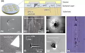
Silicon Carbide (SiC), as a third-generation wide-bandgap semiconductor material, has gained significant importance in power electronics, including electric vehicles, photovoltaic inverters, high-voltage power supplies, and industrial energy systems. Thanks to its wide bandgap, high breakdown electric field, and excellent thermal conductivity, SiC enables devices with higher efficiency, higher switching speed, and better high-temperature stability compared […]
N-Type vs. Semi-Insulating SiC Wafers: Main Differences and Applications

Silicon carbide (SiC) wafers have become one of the most important wide-bandgap semiconductor substrates in power electronics, RF communication, and high-temperature applications. Among the most widely used types are N-type SiC wafers and semi-insulating SiC wafers. Although they may look similar physically, their electrical behavior and application fields are fundamentally different. Choosing the wrong type […]
Why Advanced SiC Manufacturing Matters: Complexity Drives Technology Leadership
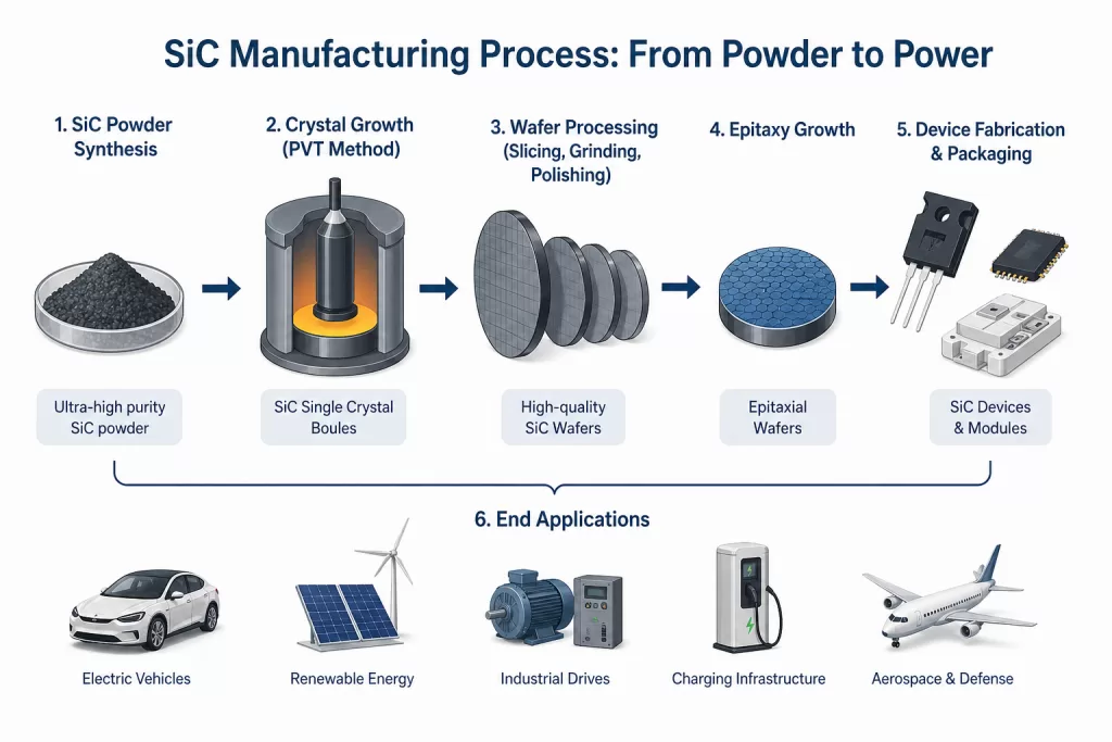
Silicon carbide (SiC) has rapidly become one of the most critical materials in modern semiconductor technology. As industries shift toward high-efficiency power electronics, electric vehicles (EVs), renewable energy systems, and high-frequency devices, the demand for high-quality SiC wafers continues to surge. However, one reality remains clear:the more complex the SiC process, the more critical advanced […]
Why Silicon Carbide Substrates Have Become a “Must-Have Material” for New Energy and 5G
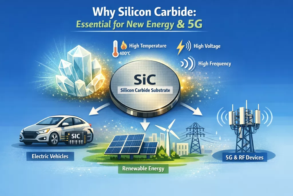
1. Introduction: From Silicon Limits to Wide Bandgap Breakthroughs As global industries accelerate toward electrification and digitalization, conventional silicon (Si)-based semiconductors are approaching their physical and performance limits. Applications such as electric vehicles, renewable energy systems, and 5G communications demand devices that can operate under higher voltages, higher temperatures, and higher frequencies. In this context, […]
Custom SiC Wafer Solutions: From Sizes to Doping
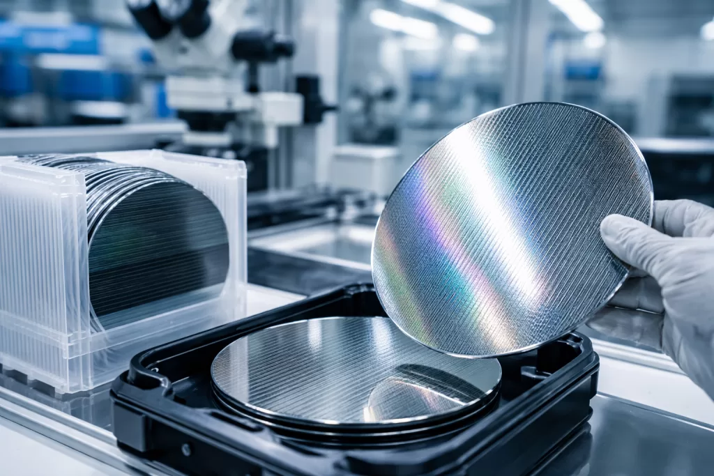
SiC wafer have become a foundational material in modern power electronics and high-frequency devices, driven by their superior physical and electrical properties. Compared with conventional silicon, SiC exhibits a wide bandgap (~3.26 eV for 4H-SiC), high thermal conductivity, and a strong critical electric field, enabling devices to operate efficiently under high voltage, high temperature, and […]
What Are the Carbon Face and Silicon Face of a Silicon Carbide Wafer?
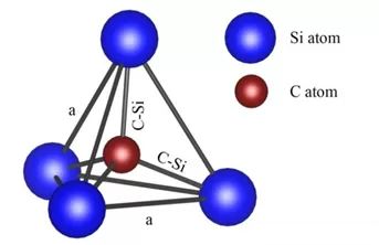
In modern power electronics, Silicon Carbide has become one of the most important wide-bandgap semiconductor materials. Compared with traditional Silicon, SiC offers superior properties such as higher breakdown electric field, better thermal conductivity, and the ability to operate at higher temperatures and voltages. Because of these advantages, SiC is widely used in power devices for […]
300mm vs. 200mm SiC Wafer Cost Analysis: At What Production Volume is the 12-Inch Transition Profitable?
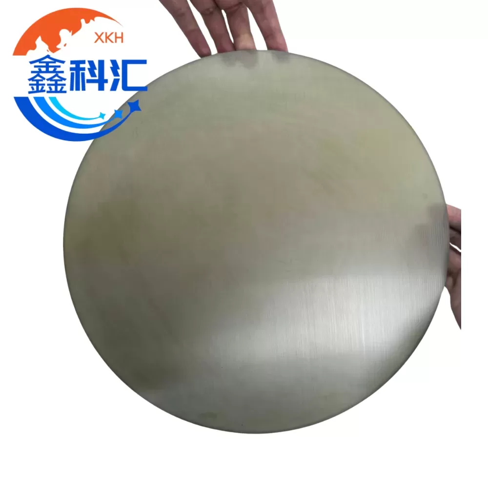
Silicon carbide (SiC) wafers have become a critical material for high-power electronics, electric vehicles, and advanced semiconductor devices. As the demand for higher efficiency, smaller form-factor devices grows, semiconductor manufacturers face a strategic decision: whether to transition from conventional 200mm (8-inch) SiC wafers to 300mm (12-inch) wafers. While larger wafers promise cost savings per device, […]
300mm SiC Wafers Challenges: The Technical Hurdles of Crystal Growth in Larger Diameters (EFG vs. PVT)
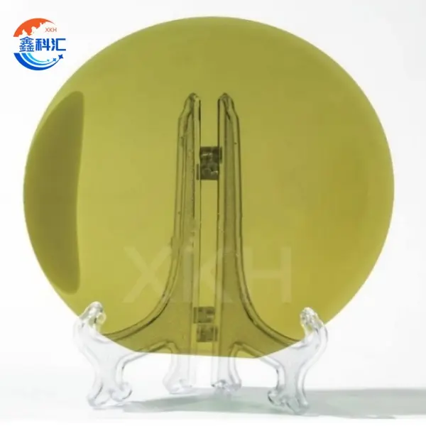
Silicon carbide (SiC) has emerged as a cornerstone material for high-power electronics, electric vehicles, and next-generation semiconductor devices due to its exceptional thermal conductivity, high breakdown voltage, and chemical stability. As the semiconductor industry pushes for larger wafer diameters to reduce production costs and increase throughput, the transition from conventional 150mm and 200mm SiC wafers […]