
SiC Wafer Market in 2026: Why Price Is Giving Way to Yield, Quality and 200 mm Qualification
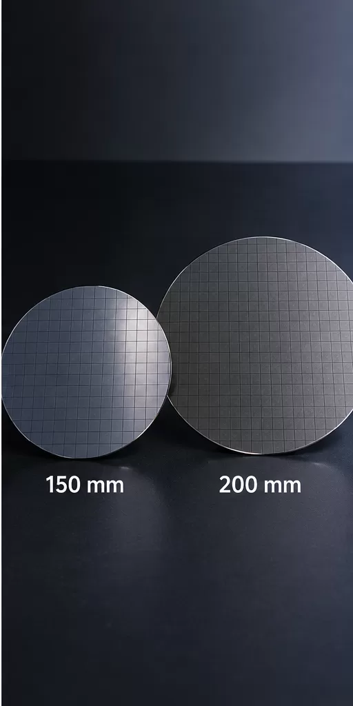
For much of the recent silicon carbide cycle, the discussion around SiC wafers was dominated by two subjects: capacity and price. Suppliers added crystal-growth capacity, Chinese manufacturers expanded aggressively, 150 mm substrate prices declined, and almost every major SiC producer announced a roadmap toward 200 mm production. In 2026, however, the market is entering a […]
Laser Stealth Dicing of SiC Wafers: Subsurface Microcracks, Edge Chipping, Dicing Quality, Inspection and Yield Control
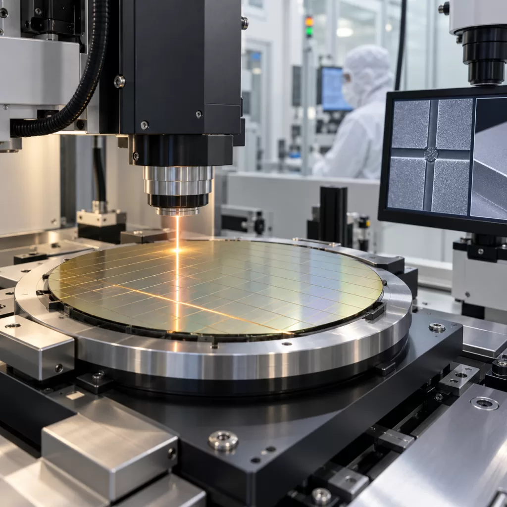
Silicon carbide wafers are increasingly used in high-power and high-temperature semiconductor devices, but they also present major challenges during singulation. Because SiC is extremely hard and brittle, conventional blade dicing can cause edge chipping, kerf loss, mechanical stress and tool wear. As device structures become smaller and wafer value increases, manufacturers are paying more attention […]
Thin SiC Wafer Handling from Backgrinding to Dicing: Ring Frame Mounting, Tape Stress, Warpage and Edge Chipping Control
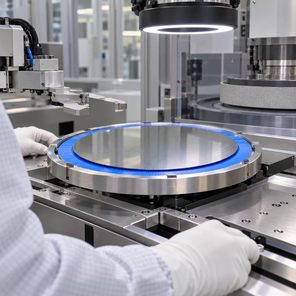
As silicon carbide wafers move toward thinner substrates for power semiconductor manufacturing, wafer handling becomes increasingly important. A standard SiC wafer may remain relatively rigid during conventional processing, but after backgrinding, the reduction in thickness significantly increases sensitivity to bending stress, local pressure, tape tension and mechanical impact. For thin SiC wafers, the transition from […]
Wafer Ring Frame Specification Guide: Sizes, Materials, Dicing Tape Compatibility and SiC Wafer Handling
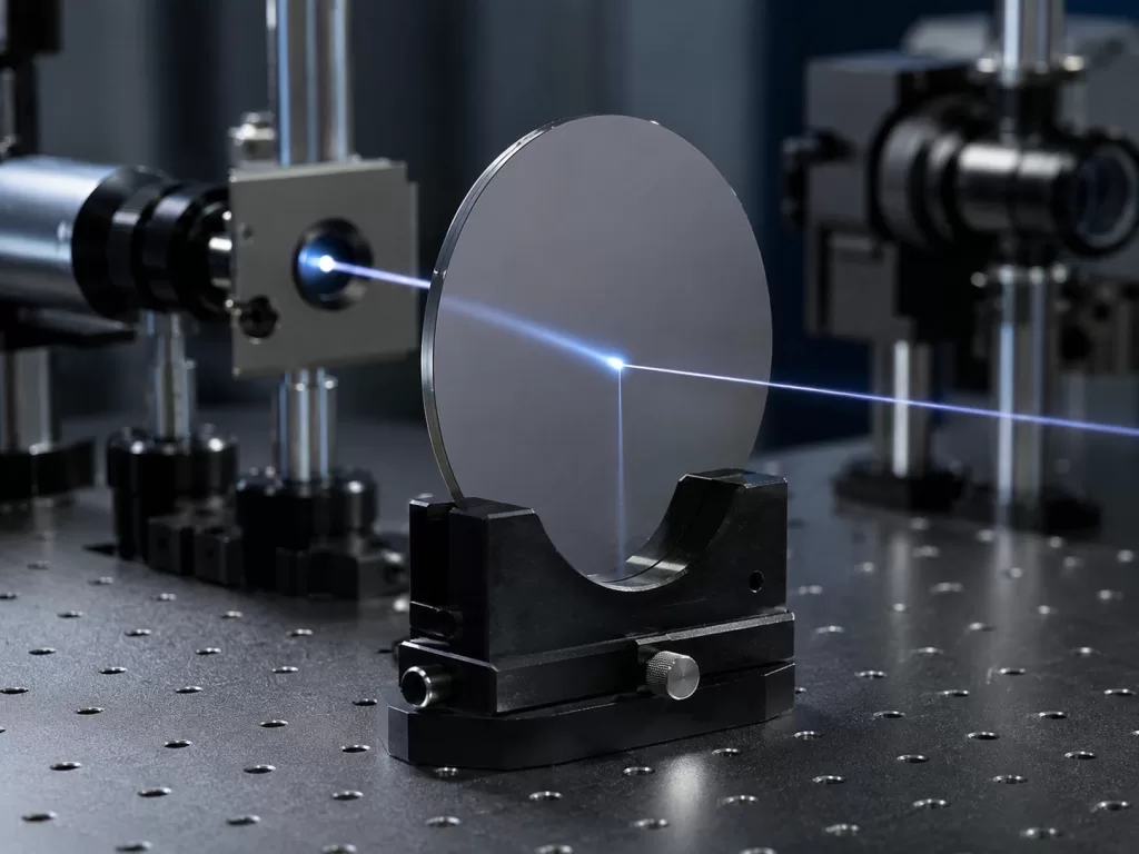
Wafer ring frames, also called dicing frames, tape frames, or wafer frames, are widely used to support semiconductor wafers during dicing, grinding-related handling, cleaning, inspection, die separation, and downstream packaging processes. Although the frame itself is mechanically simple, incorrect frame dimensions, insufficient rigidity, poor tape compatibility, or improper wafer mounting can cause alignment errors, tape […]
8-Inch SiC Wafer Specifications: Diameter, Thickness, Resistivity and Defect Limits
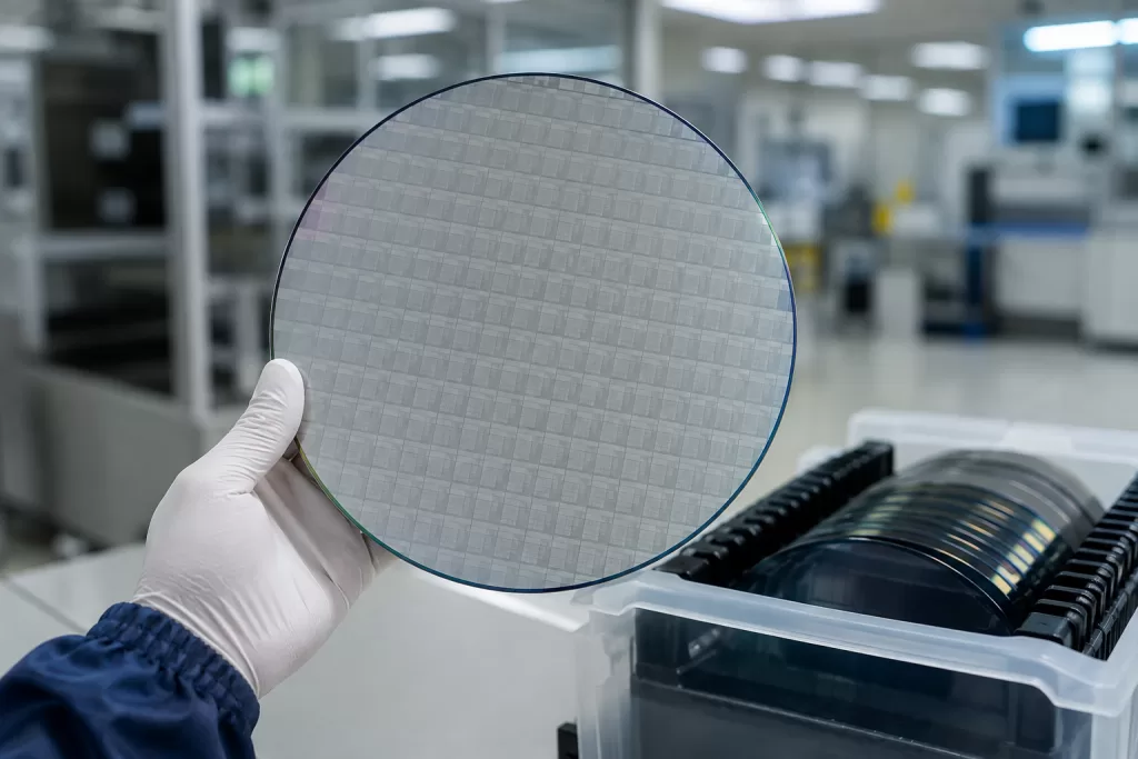
Silicon carbide (SiC) has become one of the most important semiconductor materials for high-power, high-voltage and high-frequency applications. As electric vehicles, renewable energy systems, AI power supplies and industrial automation continue to grow, the demand for larger SiC substrates is increasing rapidly. Compared with traditional 6-inch wafers, 8-inch (200 mm) SiC wafers provide more usable […]
Why Global Demand for SiC Wafers Continues to Grow Across EV, Renewable Energy and Industrial Electronics

Silicon carbide wafers have moved from a specialized semiconductor material to a strategically important foundation for modern power electronics. The strongest demand comes from electric vehicles, renewable energy infrastructure and industrial electronic systems. These sectors all face a similar engineering challenge: they must control increasingly large amounts of electrical power while reducing energy losses, thermal […]
Future Trends in SiC Wafer Manufacturing: Larger Diameters, Lower Defect Density and Higher Yield
Silicon carbide (SiC) has become one of the most important semiconductor materials for next-generation power electronics. Compared with conventional silicon, SiC offers a wider bandgap, higher critical electric field, greater thermal conductivity and superior high-temperature performance, making it the preferred material for electric vehicles (EVs), renewable energy systems, industrial motor drives, rail transportation and aerospace […]
SiC Wafer Manufacturing Challenges: Crystal Growth, Slicing, and Polishing
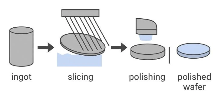
Silicon Carbide (SiC) has emerged as one of the most important semiconductor materials for next-generation power electronics. Thanks to its wide bandgap, high thermal conductivity, and superior breakdown electric field, SiC devices offer significant advantages over traditional silicon-based technologies in electric vehicles, renewable energy systems, industrial drives, and high-voltage power conversion. Despite these advantages, manufacturing […]