
1. Introduction: From Wafer Diameter to Industrial Capability
In semiconductor technology, wafer diameter has historically served as a reliable indicator of manufacturing maturity. Each major transition in wafer size—from 150 mm to 200 mm, and later to 300 mm—has marked a shift from laboratory-scale innovation to industrial-scale production. These transitions are not merely geometric expansions; they fundamentally redefine yield, cost structure, tool ecosystems, and process control methodologies.
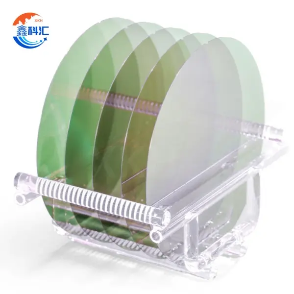
Silicon carbide (SiC), a flagship wide-bandgap semiconductor material, is now approaching a comparable transition. While SiC devices have already demonstrated decisive advantages in high-power and high-temperature applications, the widespread adoption of SiC has been constrained by substrate availability, cost, and scalability. The emergence of 300 mm SiC wafers therefore represents a critical inflection point—one that may determine whether SiC fully integrates into mainstream semiconductor manufacturing or remains a specialized material for niche markets.
2. Why 300 mm Matters More for SiC Than for Silicon
For silicon, the transition to 300 mm wafers was driven primarily by cost reduction and productivity gains in highly mature CMOS processes. For SiC, the motivation is deeper and more structural.
SiC devices typically operate at:
- Higher voltages
- Higher power densities
- Higher junction temperatures
As a result, the cost per functional die and defect tolerance are far more sensitive to substrate quality and usable wafer area than in silicon technologies. Increasing wafer diameter from 200 mm to 300 mm increases the usable surface area by approximately 125%, dramatically improving:
- Die-per-wafer yield
- Statistical averaging of defect distributions
- Cost efficiency of epitaxy, lithography, and metrology steps
In this sense, 300 mm wafers are not merely advantageous for SiC—they are a prerequisite for its long-term economic viability at scale.
3. Crystal Growth at 300 mm: Fundamental Physical Constraints
3.1 Scaling Physical Vapor Transport (PVT)
Bulk SiC substrates are predominantly grown using physical vapor transport (PVT), a process characterized by extreme temperatures, steep thermal gradients, and complex gas-phase chemistry. Scaling PVT from 150–200 mm to 300 mm boule diameters introduces several non-linear challenges:
- Radial thermal gradients increase significantly with diameter
- Supersaturation uniformity becomes increasingly difficult to maintain
- Stress accumulation during cooldown intensifies
At 300 mm scale, even minor thermal asymmetries can translate into macroscopic wafer bow, crystallographic tilt, or localized defect clustering.
3.2 Defect Evolution and Control
Defect control remains the defining challenge for large-diameter SiC wafers. Critical defects include:
- Micropipes
- Basal plane dislocations (BPDs)
- Threading screw and edge dislocations
While micropipe densities have been dramatically reduced over the past decade, maintaining low BPD densities across a 300 mm wafer requires precise control of seed quality, growth kinetics, and thermal field symmetry. The statistical impact of even low defect densities becomes more pronounced as wafer area increases, elevating the importance of advanced inspection and defect mapping.
4. Wafering, Surface Engineering, and Mechanical Stability
SiC’s exceptional hardness and brittleness introduce unique challenges in wafering and surface preparation, especially at large diameters.
At 300 mm scale:
- Mechanical slicing induces higher residual stress
- Edge integrity becomes more difficult to preserve
- Subsurface damage propagates over larger areas
Achieving epi-ready surfaces requires a tightly controlled combination of grinding, lapping, and chemical mechanical polishing (CMP). Surface roughness, damage depth, and crystallographic uniformity directly impact epitaxial layer quality and, ultimately, device reliability.
Moreover, wafer flatness and warp control become critical for compatibility with advanced lithography and automated handling systems originally designed for silicon wafers.
5. Epitaxy on 300 mm SiC: Uniformity at Scale
Epitaxial growth is the functional heart of SiC device manufacturing. Transitioning epitaxy processes to 300 mm wafers introduces stringent requirements on:
- Thickness uniformity
- Dopant concentration control
- Interface abruptness
Small variations that are tolerable at 150 mm scale can lead to unacceptable device parameter spread at 300 mm. This places significant demands on reactor design, gas flow modeling, and real-time process monitoring.
The successful scaling of epitaxy is therefore inseparable from the successful commercialization of 300 mm SiC substrates.
6. Equipment Ecosystem and Process Integration
One of the most profound implications of 300 mm SiC wafers is their alignment with existing 300 mm silicon fabrication infrastructure. While SiC processing imposes stricter thermal and mechanical requirements, compatibility with silicon-standard wafer handling, metrology, and automation systems offers substantial long-term benefits.
This convergence enables:
- Shared tool platforms
- Reduced capital expenditure per wafer
- Faster process learning cycles
However, it also demands that SiC wafers meet silicon-like standards in terms of flatness, thickness variation, and mechanical robustness—an exceptionally high bar for a wide-bandgap material.
7. Strategic Impact on Power Electronics and Beyond
The availability of 300 mm SiC wafers has far-reaching implications beyond incremental cost reduction. It enables:
- High-volume production of next-generation power devices
- More complex device architectures with higher integration density
- Improved reliability through tighter process control
In sectors such as electric mobility, renewable energy, and high-voltage power transmission, these advantages translate directly into higher system efficiency, reduced cooling requirements, and lower total cost of ownership.
Beyond power electronics, large-area SiC wafers also create opportunities in:
- High-temperature MEMS
- Harsh-environment sensors
- RF and microwave electronics
8. Outlook: Toward a Mature SiC Manufacturing Paradigm
The transition to 300 mm SiC wafers is neither immediate nor trivial. It requires coordinated progress across crystal growth, wafer processing, epitaxy, and equipment ecosystems. Nevertheless, the trajectory is clear: wafer scaling is the most direct path toward transforming SiC from a high-performance specialty material into a foundational semiconductor platform.
As technical barriers are progressively overcome, 300 mm SiC wafers are poised to play a central role in the next generation of energy-efficient and high-reliability electronic systems.
9. Conclusion
300 mm silicon carbide wafers represent a pivotal milestone in the evolution of wide-bandgap semiconductors. More than a dimensional upgrade, they embody the convergence of materials science, manufacturing engineering, and industrial strategy. Their successful deployment will define the pace and scope of SiC adoption across power electronics, sensing, and advanced semiconductor applications, shaping the technological landscape for decades to come.