
1. Introduction
Silicon has dominated the semiconductor industry for decades due to its abundance, stable crystalline structure, and excellent electronic properties. However, as device scaling approaches physical limits and applications demand higher performance, alternative materials are increasingly being explored. These new materials aim to overcome the limitations of silicon in areas such as high-power electronics, high-frequency communication, optoelectronics, and next-generation computing.
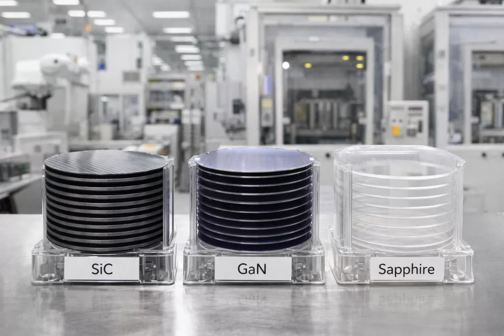
Among these alternatives, Sapphire substrates (Al₂O₃) have gained prominence, particularly as the foundational material for GaN-based devices and high-performance LEDs. Their high thermal and chemical stability, along with optical transparency, make them indispensable in certain semiconductor manufacturing processes.
2. Wide-Bandgap Semiconductors and Sapphire Substrates
Wide-bandgap (WBG) semiconductors are materials with larger bandgaps than silicon (1.1 eV), making them suitable for high-power, high-temperature, and high-frequency applications.
2.1 Silicon Carbide (SiC)
Silicon carbide has become a leading material in power electronics, especially for electric vehicles, renewable energy systems, and industrial applications. Its properties include:
- High breakdown voltage and thermal conductivity
- Low switching losses for high-efficiency power conversion
- Operation at temperatures exceeding 200°C
High-quality SiC wafers (SiC substrates) form the base for manufacturing MOSFETs, Schottky diodes, and power modules. These wafers are essential for achieving high efficiency, compact designs, and reliability in next-generation power devices.
2.2 Gallium Nitride (GaN)
Gallium nitride is widely used for high-frequency RF amplifiers, high-brightness LEDs, and emerging power electronics. Its advantages over silicon include:
- High electron mobility and saturation velocity
- High breakdown voltage
- Capability to operate efficiently at high frequencies
Many GaN devices are grown on sapphire substrates, which provide a stable and optically transparent platform for epitaxial growth. Sapphire’s lattice structure, chemical stability, and thermal robustness make it ideal for GaN epitaxy, enabling high-performance LEDs, RF devices, and optoelectronic components.
2.3 Sapphire Substrates (Al₂O₃)
Sapphire substrates are primarily used in GaN-based devices, but their role is expanding as the demand for high-quality optoelectronics grows. Key characteristics include:
- Excellent thermal conductivity for heat dissipation
- High chemical and mechanical stability under fabrication processes
- Optical transparency across a wide wavelength range
- Compatibility with large-area epitaxial growth
Sapphire substrates allow the production of high-brightness LEDs, laser diodes, and RF devices with consistent quality. Advances in substrate polishing, defect reduction, and wafer size scaling (up to 6 inches and beyond) are improving yield and reducing costs, which is crucial for mass adoption in lighting and display technologies.
3. Compound Semiconductors
Beyond WBG materials, other compound semiconductors remain important for specialized functions:
3.1 Gallium Arsenide (GaAs)
GaAs is widely used in high-frequency RF and optoelectronic devices due to its direct bandgap and high electron mobility. Applications include:
- 5G communication and satellite transceivers
- High-efficiency photovoltaic cells
- High-speed lasers and modulators
3.2 Indium Phosphide (InP)
InP is essential for fiber-optic communication and high-speed photonic circuits. Its advantages include:
- High electron mobility and low noise
- Direct bandgap suitable for infrared applications
- Integration into high-speed optoelectronic devices
4. Two-Dimensional and Oxide Semiconductors
Two-dimensional materials such as graphene, MoS₂, and hexagonal boron nitride offer atomically thin structures with high mobility and flexibility, enabling ultra-scaled transistors and flexible electronics.
Oxide semiconductors, such as IGZO, are used in transparent thin-film transistors for displays, offering:
- High electron mobility
- Optical transparency
- Low-temperature processing compatibility
These materials complement WBG semiconductors and sapphire substrates in specialized applications such as flexible displays and wearable devices.
5. Integration and System-Level Innovation
Sapphire substrates, SiC wafers, and GaN devices are increasingly integrated into high-efficiency modules:
- Compact inverters and power modules for electric vehicles
- High-brightness LEDs and laser diodes
- Advanced thermal management solutions for high-power applications
This integration maximizes efficiency, reliability, and performance across industrial, automotive, and optoelectronic systems.
6. Challenges and Industry Outlook
Despite their advantages, emerging semiconductor materials face challenges:
- High production costs, particularly for SiC and sapphire substrates
- Lattice mismatch and thermal expansion differences
- Manufacturing scalability and defect control
Continued research focuses on improving wafer quality, scaling production, and integrating alternative materials with conventional silicon processes. Sapphire substrates remain critical for GaN devices, while SiC wafers are essential for power electronics, illustrating the importance of material selection in semiconductor innovation.
7. Conclusion
As silicon approaches its physical and operational limits, a diverse set of alternative semiconductor materials is gaining prominence. Sapphire substrates provide a stable and optically transparent platform for GaN and other optoelectronic devices, while SiC and GaN enable high-power and high-frequency applications. Compound semiconductors, two-dimensional materials, and oxide semiconductors further expand the performance envelope. Integrating sapphire substrates, SiC wafers, and other advanced materials into semiconductor manufacturing is essential for developing efficient, scalable, and reliable next-generation electronics.