
Opis
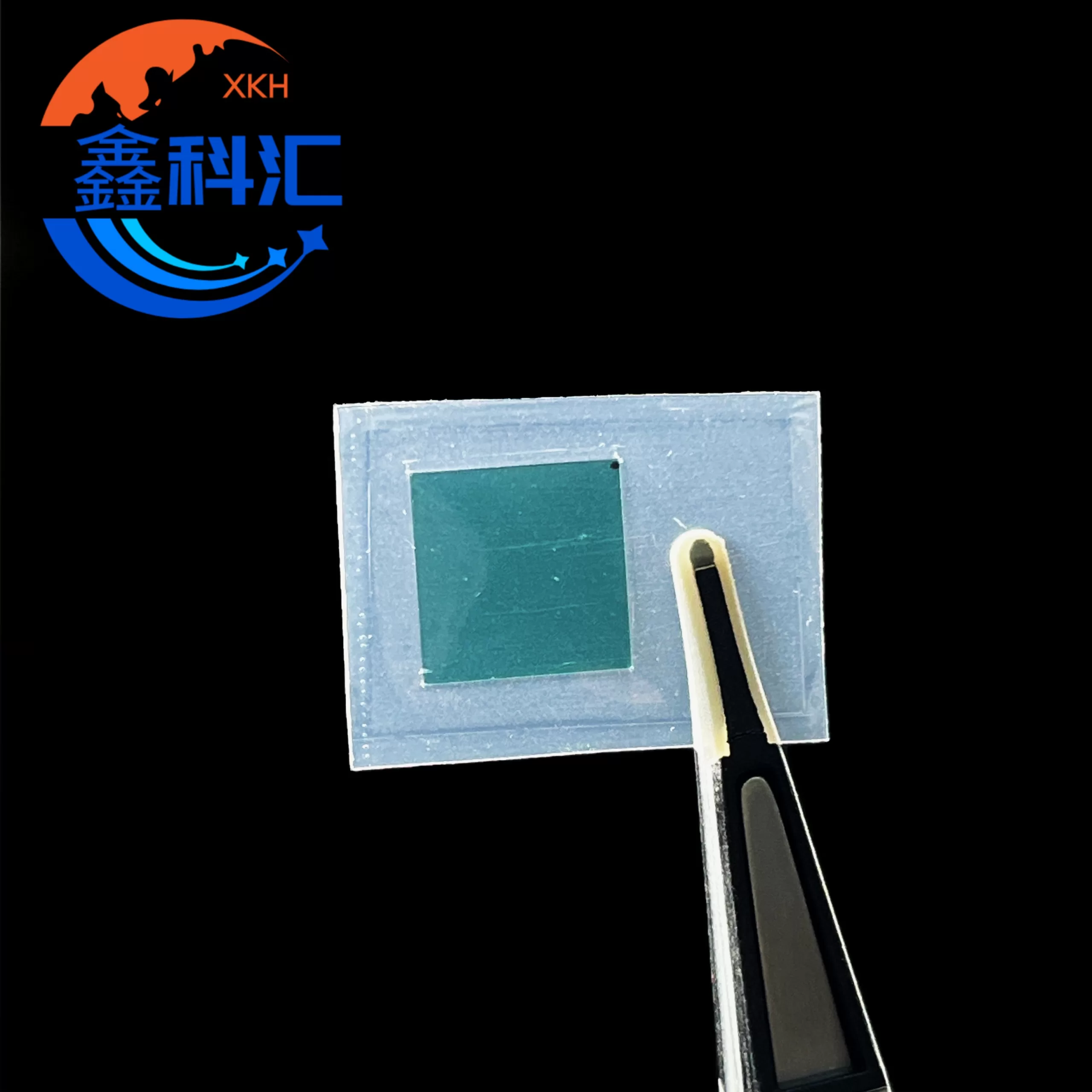
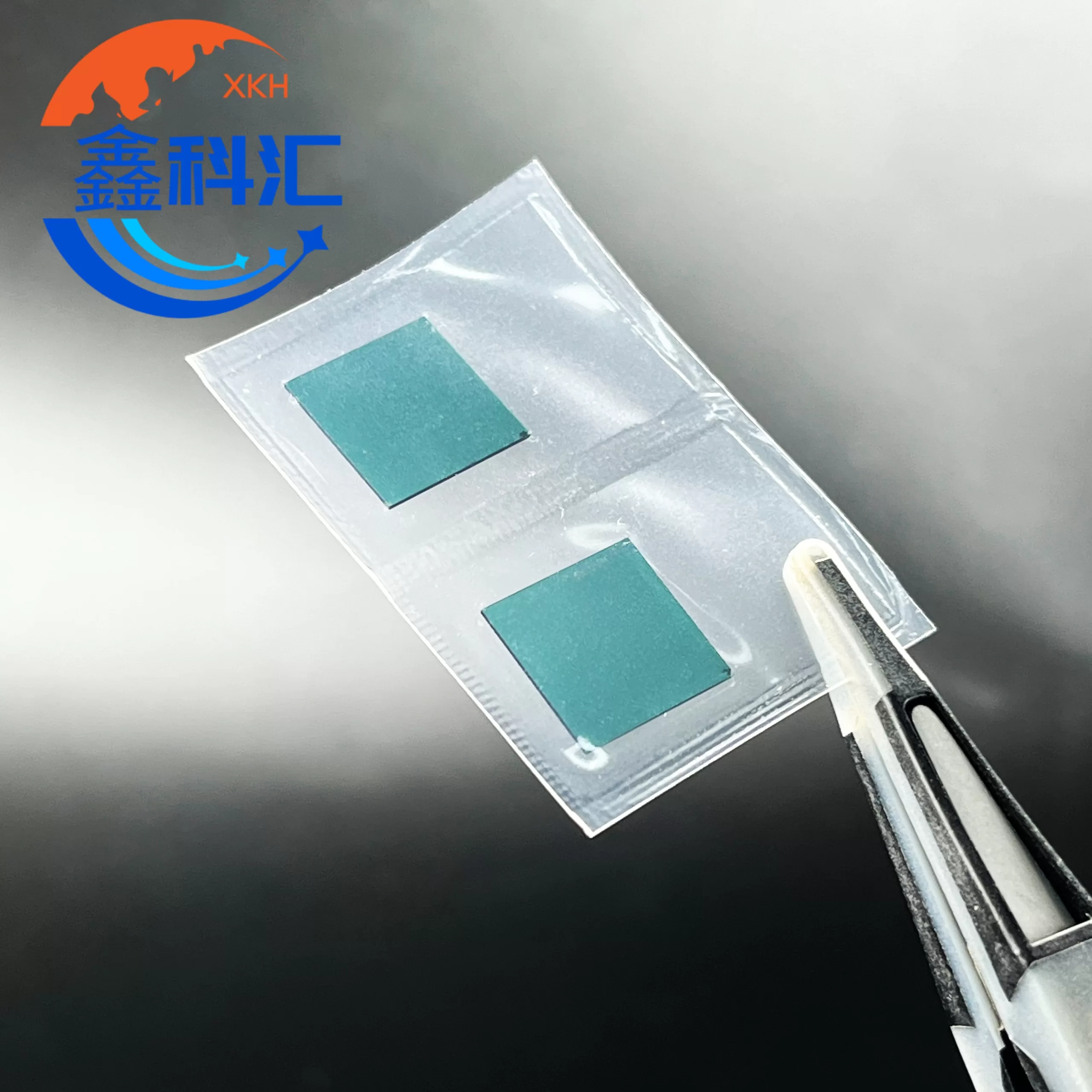
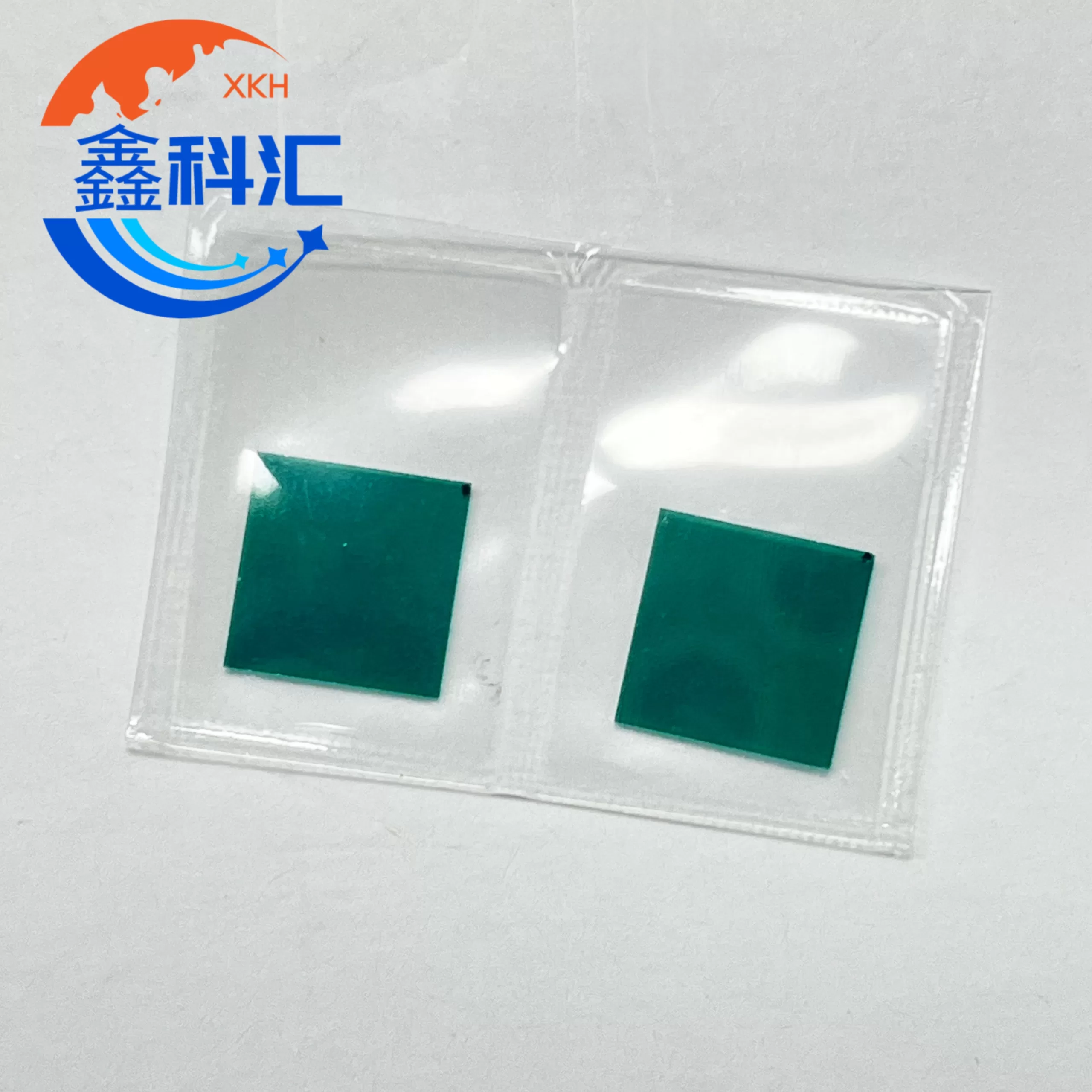
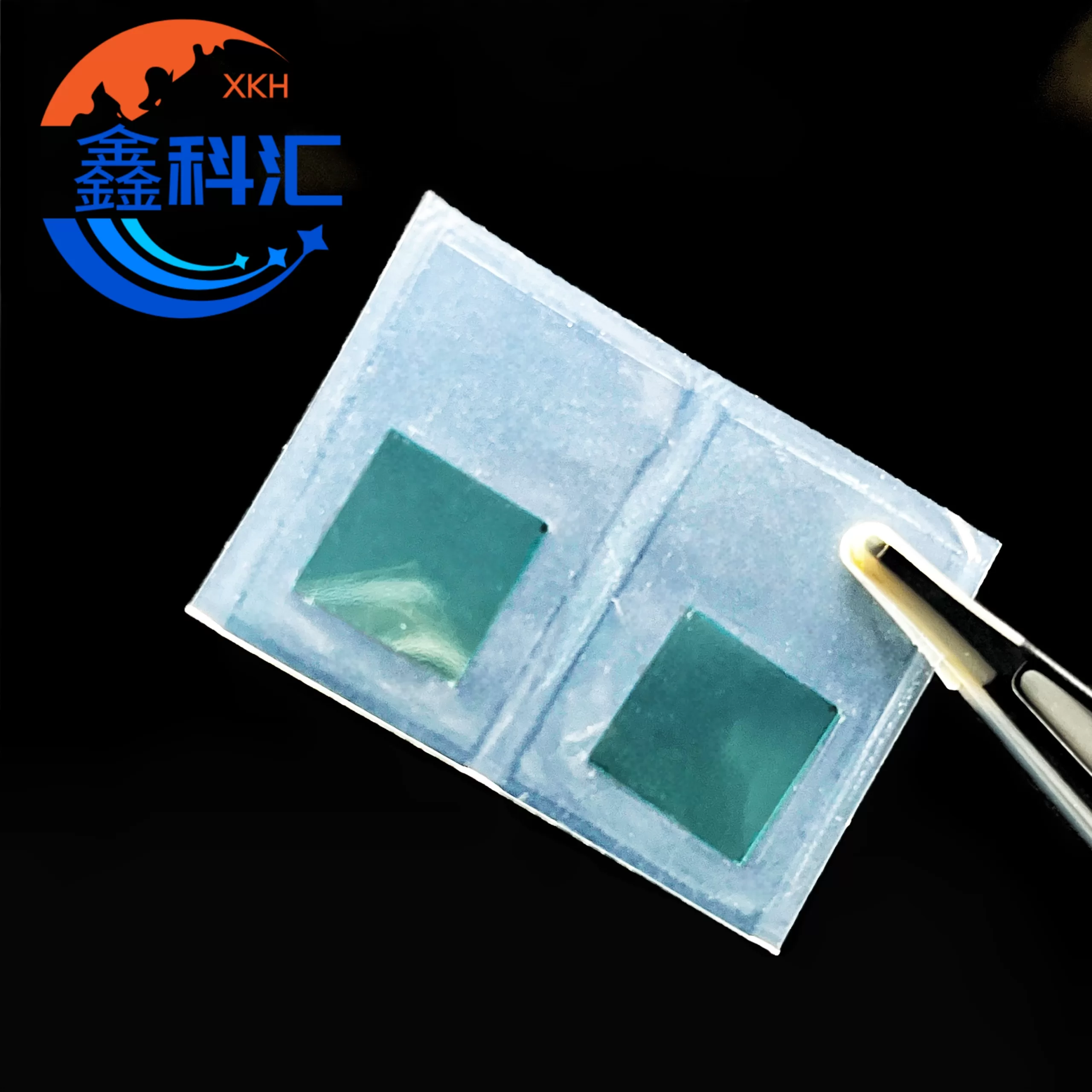
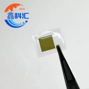
Industrial-grade 6H-N Silicon Carbide (SiC) substrates are high-quality single-crystal wafers engineered for high-temperature, UV optoelectronic, oraz precision industrial electronic applications.
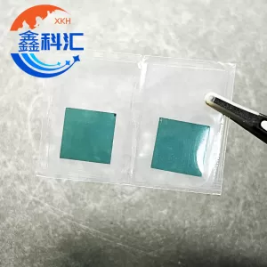
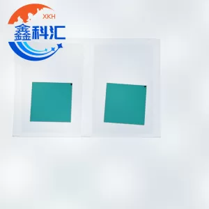
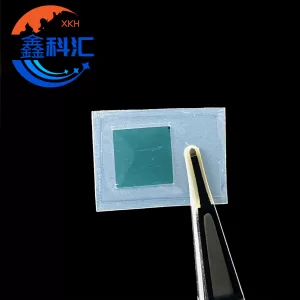
Compared with the widely used 4H SiC polytype, 6H SiC features excellent thermal stability, mechanical hardness, and cost advantages, making it ideal for UV LEDs, high-temperature sensors, aerospace electronics, and industrial-grade power components.
Kluczowe cechy
6H Hexagonal Crystal Structure
Offers dimensional stability, mechanical strength, and reliable performance under high thermal stress.N-Type Conductivity
Suitable for high-temperature electronics, UV devices, and specialized power circuits.High Thermal Conductivity (≈390–450 W/m·K)
Ensures efficient heat removal and enhances device lifetime.Superior Mechanical & Chemical Durability
High hardness, corrosion resistance, and robustness during processing.Epi-Ready Surface Options
CMP, DSP, and SSP finishes available for epitaxial growth and R&D.Customizable Sizes & Thickness
Standard diameters and square formats available for flexible integration.
Zastosowania
High-temperature semiconductor devices and industrial sensors
UV LEDs, UV detectors, and optoelectronic modules
Aerospace and automotive electronics exposed to extreme conditions
Compact, robust industrial power devices
R&D and pilot-scale production in wide-bandgap semiconductors
Technical Specifications (Typical & Customizable)
| Parametr | Specyfikacja |
|---|---|
| Materiał | Single-Crystal 6H-N SiC |
| Struktura krystaliczna | Hexagonal (6H) |
| Diameter / Size | 25 mm, 50 mm, 100 mm, 150 mm, 200 mm, 300 mm; square or custom |
| Grubość | 350–1,000 µm (customizable) |
| Wykończenie powierzchni | CMP epi-ready, DSP, SSP |
| Total Thickness Variation (TTV) | ≤5 µm typical |
| Bow / Warp | ≤40 µm (6″ typical) |
| Gęstość mikrorurek | <0.1 cm⁻² (premium <0.01 cm⁻²) |
| Gęstość dyslokacji | <10⁴ cm⁻² |
| Conductivity | N-type (conductive), SI optional |
| Epi-Ready | Yes — supports epitaxial growth |
Square Substrate Advantages
Enhanced electrode alignment for UV LEDs oraz czujniki wysokotemperaturowe
Improved device integration for industrial control circuits
Semi-insulating option enables RF and microwave low-loss performance
Manufacturing Process
High-purity SiC powder synthesis
Seed attachment and 6H polytype configuration
Sublimation crystal growth at 2300–2500°C
Diamond wire sawing into wafers
CMP or diamond polishing to achieve epi-ready surfaces
Optical inspection and CoA certification
Key Use Cases
High-temperature and high-voltage electronics
UV optoelectronic modules
Aerospace and defense systems
Industrial power solutions for harsh environments
Laboratory research and pilot device development
FAQ
1. What differentiates 6H-N SiC from 4H SiC?
6H-N SiC has slightly lower electron mobility but superior thermal stability and cost advantages for UV and high-temperature applications, while 4H SiC is optimized for fast, high-efficiency power devices.
2. Can 6H-N SiC operate under extreme temperatures?
Yes. It maintains structural and electrical stability at very high temperatures.
3. Are sizes and finishes customizable?
Absolutely — diameter, thickness, surface finish, and conductivity are fully customizable for R&D or mass production.
4. Which industries commonly use 6H-N SiC substrates?
UV optoelectronics, high-temperature sensors, aerospace, automotive electronics, and industrial-grade power modules.


Opinie
Na razie nie ma opinii o produkcie.