
Descrição
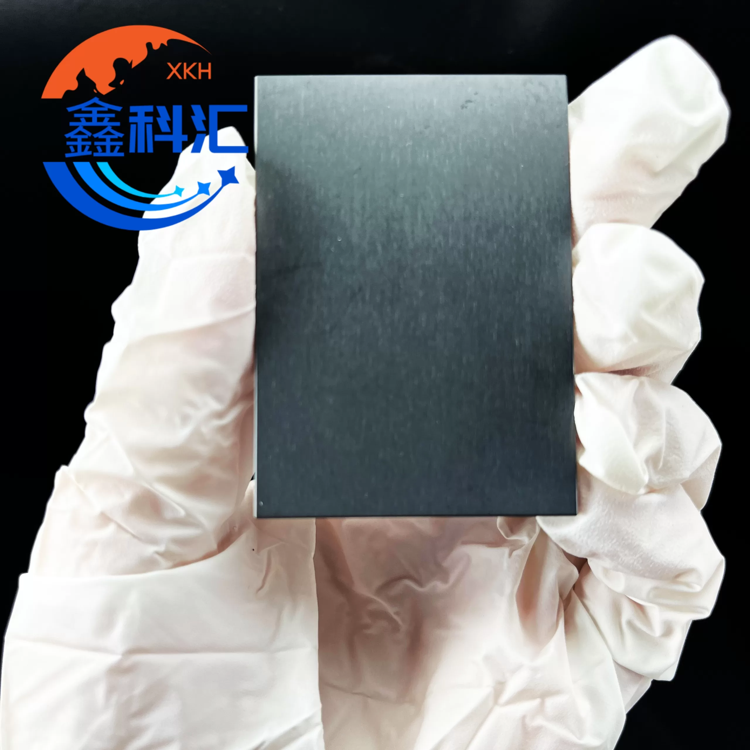
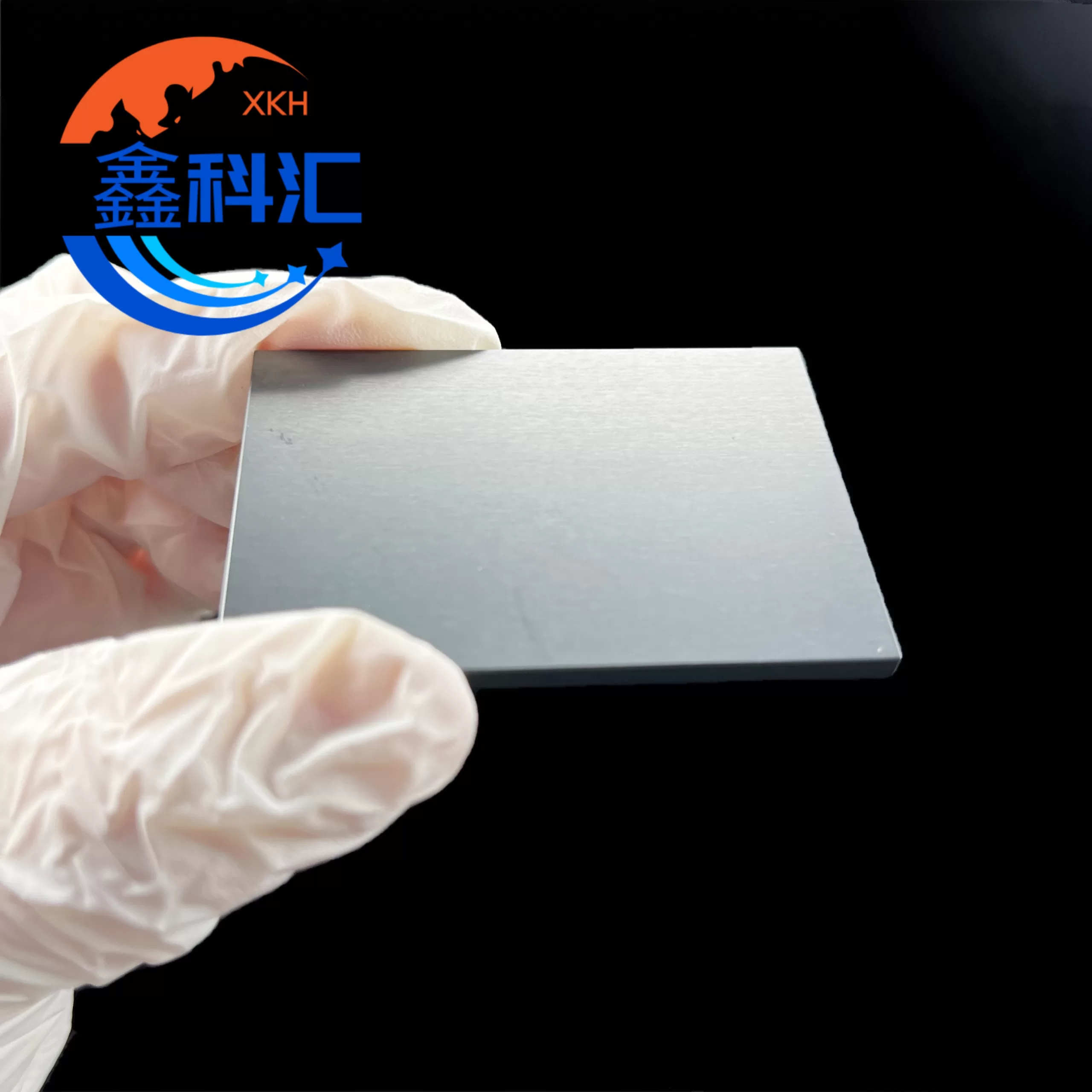
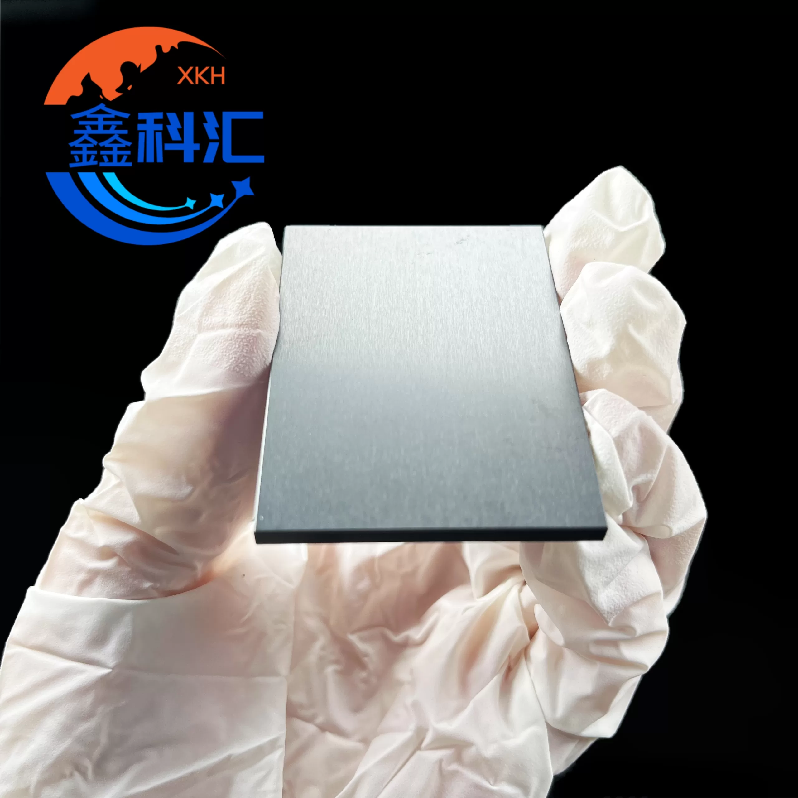
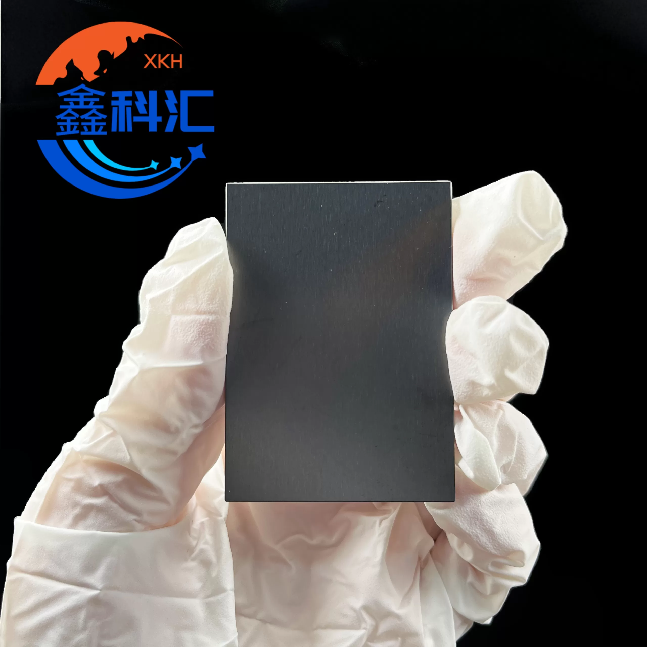
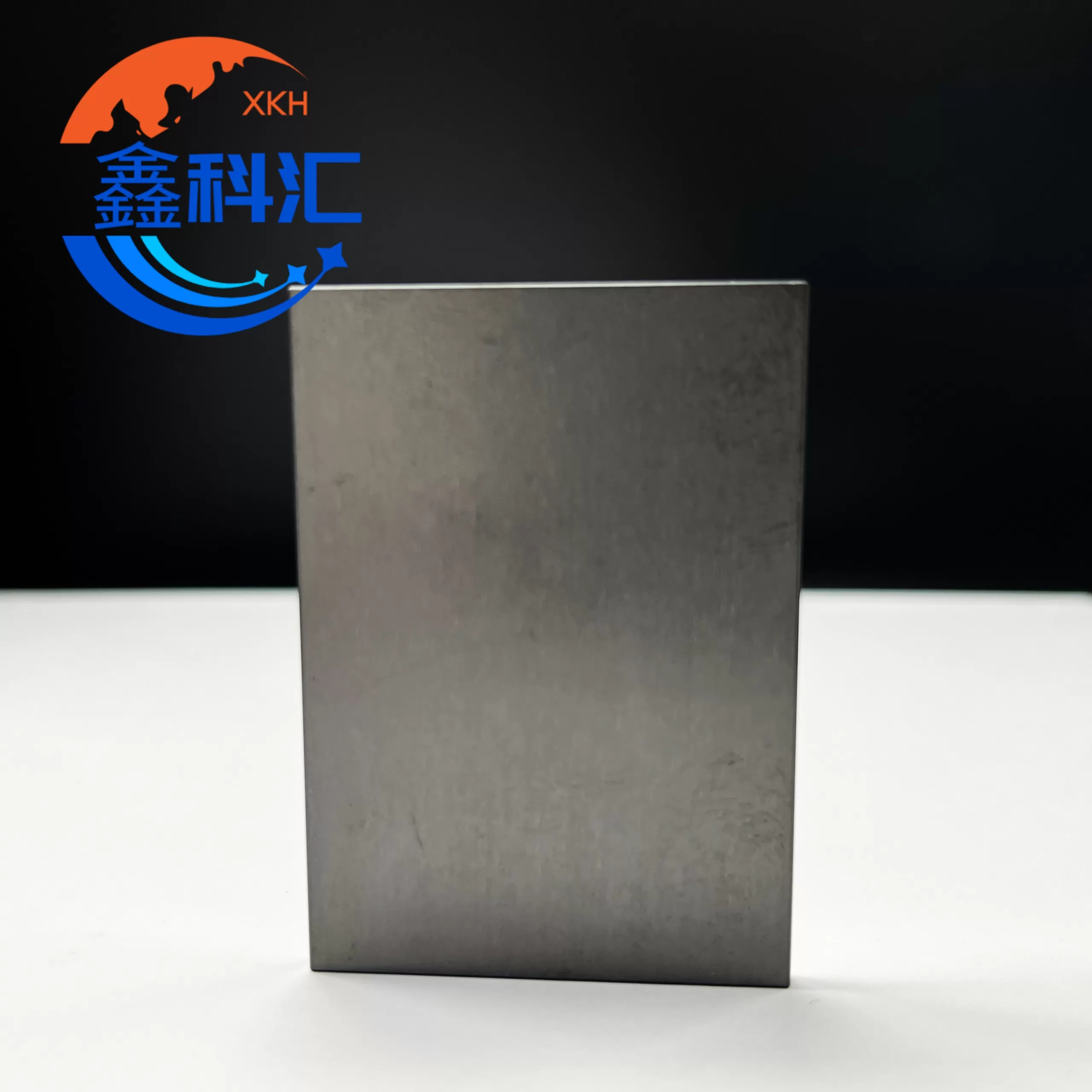
O Silicon Carbide (SiC) Rectangle Substrate is a high-performance single-crystal semiconductor material designed for next-generation electronic and photonic devices. With its wide bandgap, excellent thermal conductivity, superior chemical resistance, and high mechanical strength, SiC is widely regarded as one of the most advanced substrate materials for high-power, high-temperature, and high-frequency applications.
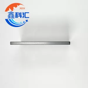
This rectangular SiC substrate offers flexible dimension customization, making it ideal for device R&D, prototype fabrication, optical components, epitaxy growth, and high-reliability industrial systems.
Key Features & Advantages
1. Wide Bandgap Semiconductor
Bandgap of ~3.2–3.3 eV, significantly higher than silicon
Supports high breakdown voltage and ultra-efficient switching performance
2. Excellent Thermal Conductivity
3.0–4.9 W/cm·K, ensuring efficient heat dissipation
Suitable for high-density power modules and RF devices
3. High Mechanical Strength
Mohs hardness ~9.2, almost as hard as diamond
Resistant to wear during wire-sawing, CMP, and device process steps
4. High-Temperature Stability
Maintains electrical and structural integrity above 600°C
Ideal for aerospace, automotive, and extreme-environment electronics
5. Customizable Dimensions & Doping
Various rectangle sizes available
N-type, P-type, semi-insulating options
Surface finish available in single / double polished, epi-ready
Manufacturing Process (PVT Growth)
Raw Material Loading
Ultra-high-purity SiC powders are placed inside a graphite crucible.Crystal Growth (>2000°C)
Using Physical Vapor Transport (PVT), SiC sublimates and recondenses on a seed crystal.Ingot Processing
The crystal boule is ground and oriented (C-plane, 0° or 4° off-axis).High-Precision Slicing
Diamond wire saws cut the crystal into rectangle plates or wafers.Lapping & Grinding
Ensures flatness, uniform thickness, and removes slicing marks.Polimento Químico-Mecânico (CMP)
Produces a mirror-grade surface suitable for epitaxial deposition.Optional Doping
Nitrogen (N-type), Aluminum/Boron (P-type), or SI/HPSI for RF & detector applications.Inspeção da qualidade
Micropipe density, warp, bow, Ra value, and TTV are fully tested.
Aplicações
Eletrónica de potência
MOSFETs de SiC
Schottky barrier diodes (SBD)
EV traction inverters
High-voltage rectifiers
RF & Microwave Devices
Radar transmitters
5G base station modules
Satellite communication systems
Optoelectrónica
UV lasers
UV photodetectors
High-power LED substrates
Extreme-Environment Electronics
Aerospace & defense
Sensores de alta temperatura
High-radiation equipment
R&D and Prototype Development
Material characterization
Epitaxial testing
Device structure optimization
Especificações técnicas
1. General Specifications
| Item | Especificação |
|---|---|
| Material | Single-crystal Silicon Carbide (SiC) |
| Shape | Rectangle substrate / plate |
| Available Polytypes | 4H-SiC, 6H-SiC |
| Orientação | C-plane (0001), Off-axis 0° / 4° |
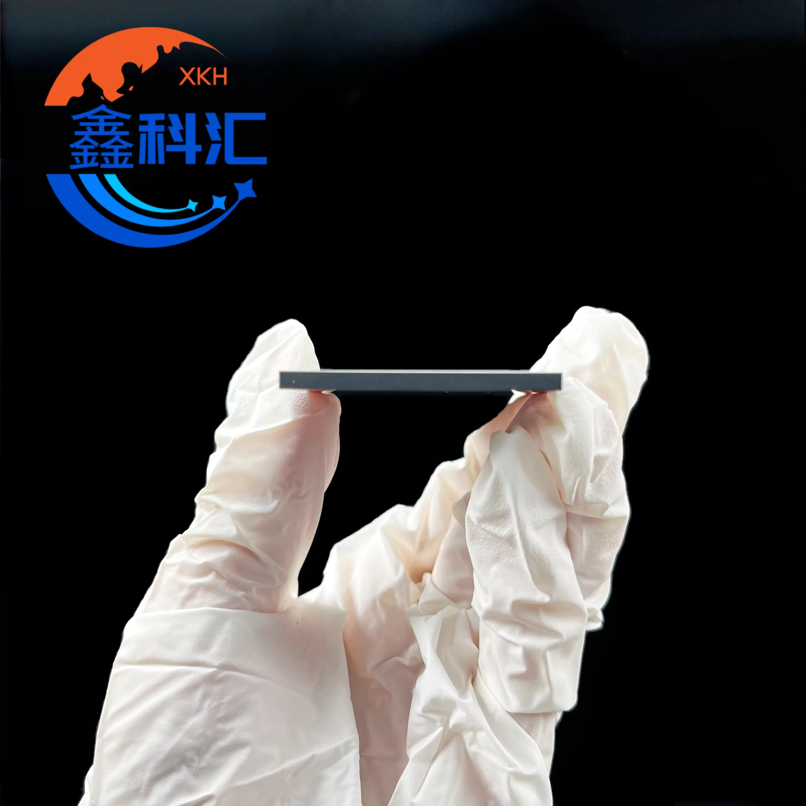
| Espessura | 330–500 μm (customizable) |
| Acabamento da superfície | SSP / DSP / Epi-ready polished |
| Doping | N-type, P-type, Semi-insulating HPSI |
| Densidade de defeitos | < 0.5 cm⁻² (4H standard), optional lower |
| Grau | Research-grade / device-grade |
2. Physical & Electrical Properties
| Imóveis | 4H-SiC | 6H-SiC |
|---|---|---|
| Bandgap | ~3.26 eV | ~3.02 eV |
| Condutividade térmica | 4.9 W/cm·K | 4.9 W/cm·K |
| Densidade | 3.21 g/cm³ | 3.21 g/cm³ |
| Breakdown Electric Field | 2.2–2.8 MV/cm | 2.2–2.8 MV/cm |
| Electron Mobility | ~800 cm²/V·s | ~400 cm²/V·s |
| Dureza de Mohs | ~9.2 | ~9.2 |
| Constante dieléctrica | 9.6 | 9.66 |
3. Surface & Quality Parameters
| Parâmetro | Valor típico |
|---|---|
| Rugosidade da superfície (Ra) | ≤ 0.2 nm (polished) |
| TTV | < 5 μm |
| Bow | < 10 μm |
| Warp | < 15 μm |
| Particle Level | < 15 @ ≥0.3 μm |
| Planicidade | λ/10 @ 632.8 nm (optional) |
4. Customization Options
| Customizable Item | Options |
|---|---|
| Dimensions | Any rectangular size available |
| Espessura | 0.33–0.50 mm standard; others on request |
| Polytype | 4H-SiC / 6H-SiC |
| Orientação | 0° or 4° off-axis |
| Polimento | SSP / DSP / Epi-ready |
| Doping | N-type, P-type, SI / HPSI |
| Edge Shape | Square edge / chamfered edge |
FAQ
Q1: Can the rectangle substrate be made in any size?
Yes. Fully customizable rectangular dimensions are available based on your design.
Q2: Do you provide epitaxy services?
We offer epi-ready polishing, and epitaxial layers can be added upon request.
Q3: What’s the typical lead time?
Standard production lead time is about 30 days.
Q4: Is research-grade and device-grade quality available?
Yes. Both grades are produced according to customer requirements.
Packaging & Delivery
Packaging: Custom anti-static boxes, vacuum-sealed or nitrogen-filled
Shipping: Protective cushioning for safe transport
Lead Time: 2-4 weeks
Supply Capability: Flexible based on order volume


Avaliações
Ainda não existem avaliações.