
SiC Wafer Market in 2026: Why Price Is Giving Way to Yield, Quality and 200 mm Qualification
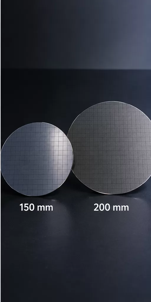
For much of the recent silicon carbide cycle, the discussion around SiC wafers was dominated by two subjects: capacity and price. Suppliers added crystal-growth capacity, Chinese manufacturers expanded aggressively, 150 mm substrate prices declined, and almost every major SiC producer announced a roadmap toward 200 mm production. In 2026, however, the market is entering a […]
SiC Epi-Wafer Uniformity for High-Temperature Electronics: Epitaxy Thickness, Doping, Defects and 6-Inch Wafer-Level Qualification
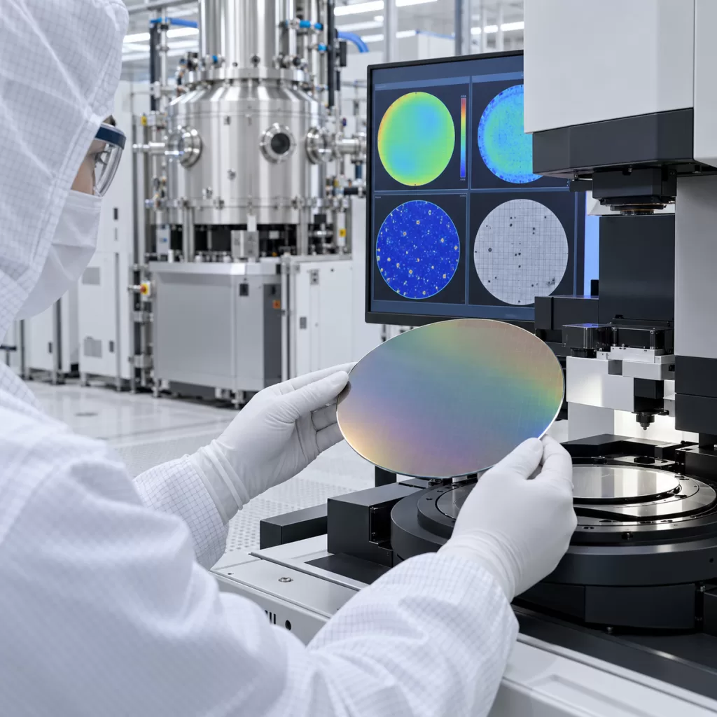
Silicon carbide is increasingly being considered for electronic systems that must operate beyond the practical temperature limits of conventional silicon electronics. Applications such as aerospace sensing, jet engines, geothermal drilling, industrial furnaces and extreme-environment monitoring require semiconductor devices that can maintain stable electrical characteristics under severe thermal conditions. For these applications, however, high-temperature performance cannot […]
300mm SiC Wafer Processing After the 12-Inch Breakthrough: Slicing, Grinding, CMP, Edge Exclusion and Yield Challenges
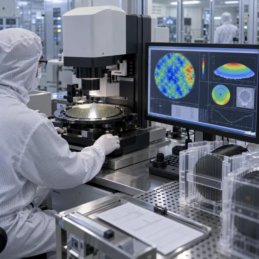
The transition of silicon carbide wafers from 150 mm to 200 mm has already forced the SiC industry to rethink crystal growth, wafer flatness, defect control and equipment compatibility. The emergence of 300 mm, or 12-inch, SiC substrates raises those challenges to an entirely different level. In September 2026, Resonac reported that it had successfully […]
How to Qualify an 8-Inch SiC Wafer Supplier in 2026: Defect Maps, TTV, Bow, Warp, Epi Quality, CoA and Lot Traceability
The transition from 150 mm to 200 mm (8-inch) silicon carbide wafers is changing how semiconductor manufacturers evaluate SiC substrate suppliers. At 150 mm, a buyer may sometimes begin qualification with basic parameters such as diameter, thickness, resistivity, surface roughness and micropipe density. For 200 mm production, that is no longer enough. As wafer diameter […]
SiC Wafer Backgrinding and Thin-Wafer Handling Guide: Thickness Control, Chipping, Warpage and Temporary Carriers
As silicon carbide devices move toward higher power density, thinner packages, and more advanced integration, wafer thinning has become an increasingly important step in SiC device manufacturing. Compared with conventional silicon, silicon carbide is significantly harder and more brittle. These properties make SiC attractive for high-power and high-temperature applications, but they also create additional challenges […]