
Silicon carbide is increasingly being considered for electronic systems that must operate beyond the practical temperature limits of conventional silicon electronics.
Applications such as aerospace sensing, jet engines, geothermal drilling, industrial furnaces and extreme-environment monitoring require semiconductor devices that can maintain stable electrical characteristics under severe thermal conditions.
For these applications, however, high-temperature performance cannot depend only on the intrinsic properties of SiC.
The quality and uniformity of the SiC epitaxial wafer are equally important.
Variations in epitaxial thickness, carrier concentration, crystal defects and wafer geometry can translate directly into variations in device characteristics across a 150 mm wafer.
As SiC technology moves from laboratory-scale devices toward wafer-level production, epi-wafer uniformity is therefore becoming a critical qualification parameter.
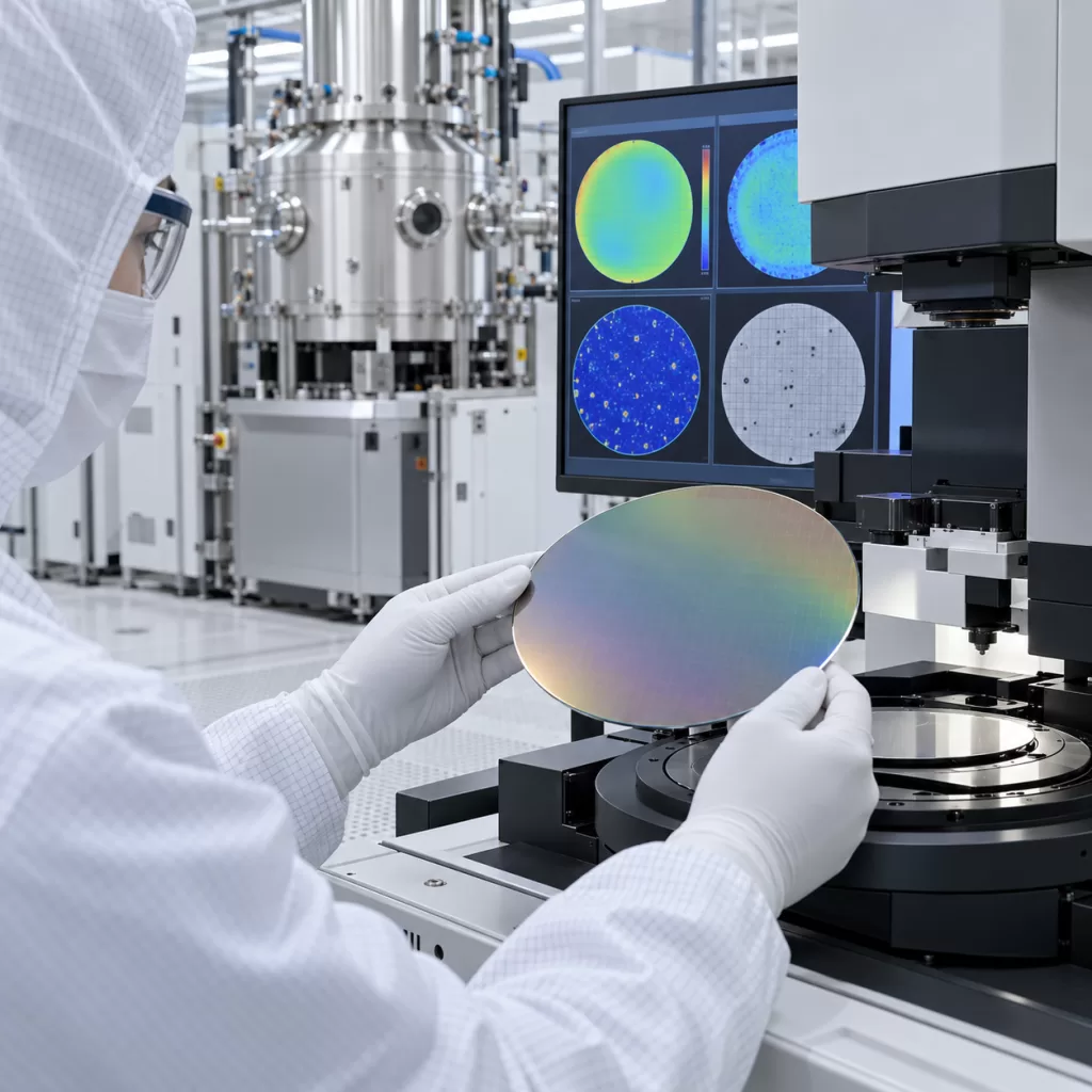
Why 6-Inch SiC Wafer-Level Uniformity Matters
A single laboratory device may perform well even if the surrounding wafer contains significant variation.
Mass production is different.
Hundreds or thousands of devices may be fabricated across the same wafer. The electrical behavior of those devices depends partly on whether the underlying epitaxial layer remains consistent from wafer center to edge.
This has become particularly relevant for high-temperature SiC electronics.
On September 28, 2026, Kyoto University reported wafer-scale fabrication of SiC junction field-effect transistors on a 6-inch SiC epi-wafer. The researchers reported high electrical uniformity in the wafer center region, with threshold-voltage standard deviation below 0.07 V. The devices are part of research targeting operation at temperatures up to 600°C.
This illustrates an important transition:
High-temperature SiC electronics are moving from demonstrating individual devices toward demonstrating repeatable performance across an entire wafer.
For epi-wafer suppliers and device manufacturers, this makes wafer-level uniformity increasingly important.
What Is a SiC Epi-Wafer?
A SiC epi-wafer normally consists of a single-crystal SiC substrate with one or more homoepitaxial SiC layers grown on its surface.
For power-device applications, the material is commonly:
- 4H-SiC;
- N-type substrate;
- Si-face;
- controlled off-axis orientation;
- N-type epitaxial layer;
- specific epitaxial thickness;
- specified carrier concentration.
Chemical vapor deposition, or CVD, is widely used to grow the epitaxial layer.
The epitaxial layer becomes part of the active device structure, so small variations in its properties can affect electrical performance.
For this reason, evaluating only the underlying substrate is not sufficient.
The complete epi-wafer must be qualified.
1. Epitaxial Thickness Uniformity
Epitaxial thickness is one of the first parameters buyers should define.
Depending on device design, the required epi thickness may range from several micrometers to tens of micrometers or significantly thicker for high-voltage structures.
The target thickness is closely related to the required blocking voltage.
But specifying only nominal thickness is not enough.
Consider an example:
Target epi thickness: 10 µm
Two wafers may both have an average thickness of approximately 10 µm, but one may vary only slightly across the wafer while the other contains large center-to-edge variation.
For device fabrication, these wafers are not equivalent.
Important parameters therefore include:
- mean epi thickness;
- thickness tolerance;
- within-wafer thickness uniformity;
- edge exclusion;
- wafer-to-wafer repeatability;
- run-to-run repeatability.
Research on 6-inch 4H-SiC homoepitaxy has demonstrated thickness uniformity below 1% under optimized reactor conditions, illustrating the level of control achievable with carefully tuned growth processes.
Why Thickness Variation Matters
Thickness variations may affect:
- electric-field distribution;
- breakdown voltage;
- drift-layer resistance;
- device matching;
- wafer-level process consistency;
- final device yield.
For high-temperature circuits containing many devices on one wafer, consistent epi thickness contributes to consistent electrical behavior across the die population.
2. Doping Concentration and Doping Uniformity
Doping concentration is equally important.
Nitrogen is commonly used as the N-type dopant in 4H-SiC epitaxy.
The required carrier concentration depends on the device architecture and targeted electrical characteristics.
Typical specifications may therefore include:
Epi doping concentration:
for example, 1 × 10¹⁵ to several × 10¹⁶ cm⁻³, depending on the application.
But again, nominal concentration does not tell the complete story.
The concentration must remain sufficiently uniform over the usable wafer area.
Research published in 2024 demonstrated less than 3% doping non-uniformity for 6-inch N-type 4H-SiC homoepitaxy after optimization of factors including C/Si ratio, growth temperature and hydrogen flow.
Other optimized 6-inch epitaxial-growth work has demonstrated doping uniformity below 2%.
Why Doping Uniformity Matters
Carrier concentration affects device characteristics such as:
- resistivity;
- threshold-related behavior;
- breakdown performance;
- on-state resistance;
- leakage characteristics;
- device-to-device electrical variation.
For wafer-level high-temperature electronics, large doping gradients can result in different electrical behavior between devices located near the center and those near the wafer edge.
This becomes increasingly problematic when multiple transistors must operate together as part of an integrated circuit.
3. Center-to-Edge Uniformity
Averages can hide important problems.
A wafer may meet the average thickness and doping specification while still showing systematic center-to-edge variation.
That is why measurement mapping is important.
Typical measurements may use multiple positions across the wafer, including:
- center;
- mid-radius positions;
- near-edge positions;
- several angular directions.
Depending on the specification, an edge-exclusion region may be defined.
For example, commercial 6-inch SiC epi-wafer specifications may use a 5 mm edge exclusion when calculating certain thickness and doping uniformity parameters.
The measurement map can reveal patterns such as:
Center high / edge low
or:
Gas-flow-side high / opposite side low
These patterns provide useful information about the epitaxial reactor and process conditions.
4. Why C/Si Ratio Matters
The carbon-to-silicon ratio during epitaxial growth has an important influence on SiC growth behavior.
Changes in C/Si ratio may influence:
- growth rate;
- surface morphology;
- defect formation;
- nitrogen incorporation;
- carrier concentration distribution.
Studies of 150 mm SiC epitaxial growth have shown that variation in effective C/Si ratio across the reactor can contribute to carrier concentration non-uniformity.
This means doping control is not simply a matter of setting the nitrogen flow.
The complete reactor environment must be controlled.
Important variables include:
- precursor flow;
- C/Si ratio;
- nitrogen flow;
- hydrogen carrier flow;
- pressure;
- temperature;
- wafer rotation;
- susceptor configuration.
Maintaining stable conditions across a 150 mm wafer becomes more difficult than for smaller wafers because the process must remain uniform over a larger surface area.
5. Temperature Uniformity During Epitaxy
Growth temperature is another critical factor.
Small temperature differences across a wafer can influence:
- growth rate;
- dopant incorporation;
- surface morphology;
- defect formation.
For a 6-inch wafer, reactor thermal design therefore becomes especially important.
The wafer, susceptor and gas flow must work together to create a stable growth environment.
Process optimization studies on 150 mm 4H-SiC epitaxy have shown that adjustments to growth temperature and gas-flow ratios can improve both thickness and doping uniformity.
This is one reason epi-wafer qualification should examine actual wafer maps rather than relying solely on nominal reactor settings.
6. Epitaxial Defects
Uniform thickness and doping do not guarantee a high-quality epi-wafer.
Defect density must also be controlled.
Common SiC epitaxial defects may include:
- basal plane dislocations (BPD);
- stacking faults;
- triangular defects;
- carrot defects;
- pits;
- particles;
- step bunching;
- surface scratches.
Different defects have different origins and device impacts.
Some originate in the substrate and propagate into the epitaxial layer.
Others may form during epitaxial growth.
Basal Plane Dislocations
BPDs are particularly important for bipolar SiC devices because they can participate in stacking-fault expansion under electrical stress.
Therefore, customers developing high-reliability or bipolar devices may require tighter BPD specifications.
Triangular Defects
Triangular defects can create localized regions that may negatively affect device yield.
For large-diameter wafers, their position becomes important because a single large defect can render one or more die unusable.
Surface Pits
Pits and related morphology defects may interfere with device processing, especially if they occur inside active device areas.
Historical 150 mm epitaxy studies have shown that surface morphology, shallow pits, triangular defects and carrier-concentration uniformity must all be considered together when evaluating epi quality.
7. Surface Roughness
Surface roughness is another important qualification parameter.
A high-quality SiC epitaxial surface should maintain smooth step-flow morphology without severe step bunching or local rough regions.
AFM is commonly used to measure nanoscale roughness.
A typical specification may be expressed as:
Ra ≤ 0.3 nm
or another agreed value depending on measurement area and application.
Some optimized 6-inch epitaxial-growth research has reported roughness below 0.2 nm.
However, buyers should always specify:
- Ra or RMS parameter;
- scan area;
- measurement location;
- number of measurement points.
A roughness value without a defined measurement method can be ambiguous.
8. Bow and Warp After Epitaxy
Wafer geometry can change during epitaxial growth.
The final epi-wafer should therefore be evaluated for:
- bow;
- warp;
- total thickness variation;
- local flatness where required.
Excessive wafer deformation may cause problems in:
- photolithography;
- wafer chucking;
- implantation;
- deposition;
- wafer probing;
- dicing;
- automated handling.
For high-temperature device manufacturing, geometry control becomes even more important if multiple high-temperature processing steps follow epitaxy.
The buyer should therefore determine whether bow and warp specifications apply to the bare substrate or the completed epi-wafer.
9. From Material Uniformity to Device Uniformity
Ultimately, epi-wafer uniformity matters because it influences device uniformity.
This connection becomes particularly visible during wafer-level electrical testing.
Engineers may map parameters such as:
- threshold voltage;
- leakage current;
- breakdown voltage;
- on-resistance;
- saturation current;
- contact resistance.
If material properties change significantly across the wafer, corresponding patterns may appear in device measurements.
Conversely, strong device uniformity across a wafer provides evidence that substrate quality, epitaxy and fabrication processes are being controlled effectively.
The recent 6-inch SiC high-temperature transistor work from Kyoto University is important for precisely this reason: it moved from individual-device demonstrations toward wafer-level fabrication and demonstrated very small threshold-voltage variation in the central wafer region.
10. High-Temperature Electronics Put Additional Pressure on Uniformity
A device designed to operate near room temperature and one designed for several hundred degrees Celsius do not face identical reliability requirements.
At elevated temperatures, engineers must consider additional effects such as:
- carrier concentration changes;
- junction leakage;
- contact stability;
- metallization stability;
- threshold-voltage drift;
- package stress;
- long-term material degradation.
Small wafer-to-wafer or die-to-die variations can therefore become more important.
High-temperature applications may include:
Aerospace and Jet Engines
Electronics located closer to engines could reduce dependence on long wiring harnesses and remote sensing electronics.
Geothermal Exploration
Downhole equipment may experience environments where conventional silicon electronics require extensive cooling or thermal protection.
Industrial Furnaces
Sensors and control circuits operating closer to high-temperature processes may improve monitoring capabilities.
Space Exploration
Extreme-temperature environments create strong demand for semiconductor materials capable of operating beyond standard silicon temperature ranges.
The recent SiC JFET research specifically identified potential applications including jet-engine sensors, geothermal development and planetary exploration.
11. What Should Be Included in a 6-Inch SiC Epi-Wafer Specification?
A useful procurement specification should define more than simply:
“6-inch 4H-SiC epi wafer.”
A more complete specification may include:
| Parameter | Typical Information to Define |
|---|---|
| Diameter | 150 mm / 6 inch |
| Polytype | 4H-SiC |
| Surface | Si-face |
| Orientation | 4° off-axis or specified orientation |
| Substrate conductivity | N-type / semi-insulating / other |
| Substrate thickness | Customer-defined |
| Epi conductivity | N-type / P-type |
| Epi thickness | Customer-defined |
| Thickness tolerance | Required range |
| Thickness uniformity | Defined across usable area |
| Doping concentration | Target cm⁻³ |
| Doping uniformity | Defined across wafer |
| Edge exclusion | For example 3–5 mm, if applicable |
| BPD | Maximum allowable density |
| Surface defects | Defined defect limits |
| Surface roughness | Ra/RMS + AFM scan area |
| TTV | Maximum limit |
| Bow | Maximum limit |
| Warp | Maximum limit |
| Measurement map | Number and position of points |
| Inspection report | Required wafer-level data |
For high-temperature electronics or research programs, customers may also request wafer maps rather than only pass/fail certificates.
12. Wafer-to-Wafer and Run-to-Run Repeatability
One good epi-wafer does not demonstrate a stable production process.
Production qualification should also evaluate:
Within-wafer uniformity
How much does one wafer vary from center to edge?
Wafer-to-wafer uniformity
How much do wafers in the same growth run vary?
Run-to-run repeatability
Does the process produce comparable results over multiple batches?
This distinction is important for customers moving from R&D quantities to production.
A research project may initially need only several wafers.
A device manufacturer preparing for volume production needs confidence that hundreds of wafers will remain within a controlled process window.
13. Industry Standards Are Becoming More Important
As SiC moves toward larger-scale power-device manufacturing, common material specifications are becoming more formalized.
SEMI currently lists SEMI M92-0326, a specification covering 4H-SiC homoepitaxial wafers used in power-device manufacturing. Its stated purpose is to provide uniform requirements between suppliers and customers in the SiC industrial chain.
This is important for buyers because terms such as:
- epi thickness;
- doping;
- wafer geometry;
- defect inspection;
- measurement methods
must be defined consistently if data from different suppliers are to be compared meaningfully.
How Buyers Should Evaluate a SiC Epi-Wafer Supplier
When sourcing 6-inch SiC epi-wafers, buyers should ask more than:
“What is your price for a 6-inch SiC epi-wafer?”
Useful questions include:
- What epi thickness range can you provide?
- What doping concentration range is available?
- How is thickness uniformity calculated?
- How many measurement points are used?
- What edge exclusion is applied?
- How is doping concentration measured?
- What BPD and surface-defect limits are available?
- Can wafer-level defect maps be provided?
- What are the final bow and warp specifications?
- Can you provide wafer-to-wafer or lot-level uniformity data?
- Are custom epi structures available?
- Can wafers be supplied for high-temperature device R&D?
For development projects, supplying the final device requirements can also help the material supplier recommend a more appropriate epi structure.
Conclusion
As SiC electronics progress from individual laboratory devices toward wafer-level manufacturing, epi-wafer uniformity is becoming one of the most important indicators of material quality.
For 6-inch SiC epi-wafers, buyers should evaluate several parameters together:
epitaxial thickness + thickness uniformity + doping concentration + doping uniformity + defect density + surface roughness + bow/warp + wafer-level repeatability
No single parameter can fully describe epi-wafer quality.
This is particularly important for high-temperature electronics, where device consistency and reliability must be maintained under conditions far beyond those of conventional silicon electronics.
Recent wafer-scale demonstrations of SiC transistors operating in extreme-temperature environments show that the industry is moving beyond proof-of-concept devices toward manufacturing-oriented wafer-level qualification.
For customers sourcing SiC epi-wafers, defining detailed material specifications and requesting appropriate wafer-level inspection data can reduce qualification risk and improve the transition from research to device manufacturing.
ZMSH can support customized 4H-SiC substrates and SiC epi-wafer specifications, including different wafer diameters, epitaxial thicknesses, doping requirements and material inspection requirements for power semiconductor, high-temperature electronics and research applications.