
For much of the recent silicon carbide cycle, the discussion around SiC wafers was dominated by two subjects: capacity and price.
Suppliers added crystal-growth capacity, Chinese manufacturers expanded aggressively, 150 mm substrate prices declined, and almost every major SiC producer announced a roadmap toward 200 mm production.
In 2026, however, the market is entering a different phase.
The question is no longer simply whether enough SiC substrates can be produced.
The more important question is:
How much usable device yield can a substrate actually deliver?
Recent developments suggest that SiC substrate competition is gradually shifting from wafer availability and headline price toward defect density, wafer geometry, epitaxial compatibility and lot-to-lot consistency.
That change may ultimately be more important than another reduction in wafer price.
From Shortage to Oversupply — and Now to Qualification
A few years ago, SiC substrate availability was considered one of the major constraints on the power semiconductor industry.
Electric vehicles were adopting SiC traction inverters, suppliers were signing long-term agreements, and substrate companies rushed to increase crystal-growth capacity.
The picture later changed.
Rapid capacity expansion, particularly in the 150 mm segment, created significant pricing pressure. TrendForce reported earlier that falling demand growth and intensified competition caused global N-type SiC substrate revenue to decline in 2024 even as the long-term industry roadmap continued moving toward larger wafers.
By 2026, the discussion has become more nuanced.
TrendForce now describes the SiC sector as moving from capacity expansion toward technology upgrades, cost competition and 200 mm manufacturing. DIGITIMES reported in October that the substrate market is showing signs of recovery, supported by automotive, energy and AI infrastructure demand.
This matters because a recovering market does not necessarily mean a return to the old supply shortage.
Instead, the market may become more selective.
There can be abundant substrate capacity while high-quality, fully qualified material remains relatively differentiated.
Cheap SiC Wafers Do Not Automatically Mean Cheap SiC Devices
A substrate is only the starting point of a semiconductor manufacturing process.
After the bare SiC wafer is produced, it may go through epitaxial growth, photolithography, implantation, high-temperature annealing, metallization, wafer thinning, dicing, packaging and electrical testing.
A small saving at the substrate purchasing stage can therefore be meaningless if the material creates yield loss later in the process.
A simple way to look at the economics is:
Effective device cost = Total wafer processing cost ÷ Number of good die
The denominator is critical.
If two substrates have the same diameter but one produces more electrically good devices, that wafer may ultimately be cheaper even if its purchase price is higher.
This is especially important for high-voltage SiC MOSFETs.
As device area increases, the probability that a critical crystal defect intersects an individual die also becomes more important.
That is why substrate quality increasingly affects both device yield and manufacturing economics.
The 200 mm Transition Changes the Quality Equation
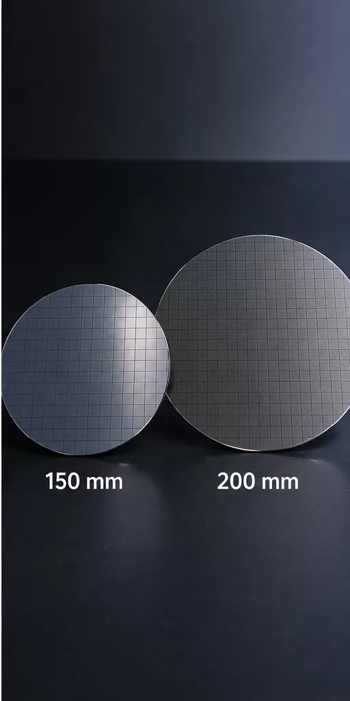
Moving from 150 mm to 200 mm offers an obvious economic attraction: more surface area and potentially more die per wafer.
But larger diameter does not make SiC crystal growth easier.
It makes it harder.
Growing a larger SiC boule requires tighter control of the thermal field, material transport, stress and crystal interface.
After crystal growth, slicing and wafer processing must also control thickness variation and wafer geometry across a larger area.
The result is that a successful 200 mm SiC program must solve two problems at the same time:
increase wafer diameter and reduce effective defect density.
If wafer diameter increases while defect control deteriorates, much of the theoretical cost advantage can disappear.
Micropipe Density Is Becoming a Commercial Metric Again
One of the clearest examples came in September 2026.
Wolfspeed announced commercial availability of a new Premium 200 mm n-type SiC substrate. Rather than focusing only on diameter, the company highlighted multiple material-quality parameters.
According to Wolfspeed, the substrate provides a micropipe density of less than 0.01 cm⁻², corresponding to fewer than three micropipes across a 200 mm wafer, based on X-ray topography. The company also reported low threading screw dislocations and emphasized wafer-shape and lot-to-lot consistency.
That announcement is important for the broader market.
It suggests that the commercial benchmark for 200 mm SiC is evolving.
Several years ago, simply demonstrating a 200 mm wafer was significant.
Now customers increasingly need information about what is actually inside that wafer.
The questions become more specific:
How many critical defects are present?
How uniform is the material across the wafer?
How stable is the wafer geometry?
How does it behave during epitaxy?
And can the supplier reproduce the same performance from lot to lot?
Wafer Shape Is Not a Cosmetic Specification
Bow and warp are sometimes treated as secondary specifications compared with defect density.
For 200 mm processing, they can be extremely important.
Modern semiconductor equipment relies on precise wafer handling and positioning.
Excessive wafer deformation can affect chucking, lithography focus, film deposition uniformity, automated transport and subsequent thermal processes.
SiC adds another challenge because many device processes involve high temperatures.
Residual stress in the substrate, combined with stress introduced by epitaxy or deposited films, can change wafer geometry during processing.
This means buyers should not evaluate only the incoming bare-wafer measurement.
They also need to understand how the wafer behaves after epitaxy and thermal processing.
For production fabs, wafer-shape stability can be more valuable than an exceptionally good measurement on a small number of selected samples.
Lot-to-Lot Consistency May Become the Real Premium Product
For research laboratories, one excellent wafer can be useful.
For mass production, it is not enough.
A power semiconductor fab may process hundreds or thousands of wafers. Engineers need the next lot to behave similarly to the previous lot.
If crystal quality, resistivity, thickness, surface condition or wafer shape varies significantly between batches, process recipes may require adjustment.
That creates additional engineering work and increases qualification risk.
As the SiC industry matures, this consistency is likely to become one of the most important differences between commodity substrates and premium production material.
The premium is therefore not simply attached to a lower number of defects.
It is attached to predictability.
150 mm SiC Is Not Disappearing
The transition to 200 mm does not mean that 150 mm SiC wafers will immediately disappear.
Existing device fabs have large installed bases of 150 mm equipment.
Many products are already fully qualified on 150 mm processes.
For mature devices and price-sensitive applications, changing wafer diameter may not provide enough economic benefit to justify new equipment, process redevelopment and customer requalification.
As a result, the SiC industry is likely to operate with both wafer sizes for an extended period.
150 mm may increasingly become a highly competitive volume platform, while 200 mm is adopted first where scale, device area, manufacturing automation and long-term cost reduction justify the transition.
This creates an interesting purchasing environment.
The cheapest wafer may not be the best option, and the largest wafer may not automatically be the best option either.
The correct substrate depends on the device design, fab platform and qualification strategy.
AI Data Centers Add a New Demand Driver
Another change in 2026 is the expanding role of AI infrastructure.
SiC demand was historically dominated by electric vehicles, renewable energy and industrial power systems.
AI data centers are adding a new high-power application.
NVIDIA is promoting an 800 VDC architecture for next-generation AI factories in order to reduce conversion stages, current, copper requirements and distribution losses. In August 2026, Wolfspeed and LITEON announced the qualification of SiC technology for LITEON’s next-generation 800 VDC power-sidecar and compute-rack PSU platforms. NVIDIA
This could have an important effect on wafer demand.
AI infrastructure does not simply require large quantities of power devices.
It requires highly reliable power conversion operating continuously at high utilization.
That places additional emphasis on device reliability and therefore on the consistency of starting semiconductor material.
Automotive qualification pushed the SiC industry toward higher quality over the previous decade.
AI power infrastructure may reinforce the same trend.
What SiC Wafer Buyers Should Evaluate in 2026
Diameter and price remain important, but they should not be considered independently.
For production-oriented purchasing, substrate evaluation increasingly needs to include crystal defect data, micropipe density, threading dislocations, resistivity uniformity, thickness and TTV, surface roughness, Bow and Warp, edge quality, epitaxial compatibility and lot-to-lot statistics.
Another important question is measurement methodology.
A specification has more value when both supplier and customer understand exactly how it is measured.
For example, defect values obtained through X-ray topography should not automatically be compared with numbers produced by another inspection technique without understanding the detection criteria.
The same principle applies to surface roughness, flatness and wafer geometry.
As the SiC market matures, documentation and measurement consistency will become nearly as important as the headline specification itself.
The Next Stage of SiC Competition
The SiC industry is not leaving cost competition behind.
Cost will remain extremely important.
But the definition of cost is changing.
The first stage of the industry focused on substrate availability.
The second stage focused heavily on wafer price.
The emerging stage will increasingly focus on cost per good device.
That shifts attention back to materials science.
Crystal growth, defect engineering, slicing, polishing, wafer geometry and epitaxial compatibility all become directly connected to device economics.
This is why the latest 200 mm substrate developments matter.
The industry is moving beyond the question:
“Can you make a 200 mm SiC wafer?”
The new question is:
“Can you repeatedly manufacture 200 mm SiC wafers that deliver predictable device yield?”
That is likely to be one of the defining competitive questions for the SiC wafer market through the remainder of 2026 and into the next phase of commercial scaling.