
Silicon carbide (SiC) has become one of the most important semiconductor materials for next-generation power electronics. Compared with conventional silicon, SiC offers a wider bandgap, higher critical electric field, greater thermal conductivity and superior high-temperature performance, making it the preferred material for electric vehicles (EVs), renewable energy systems, industrial motor drives, rail transportation and aerospace electronics.
As demand for high-performance power devices continues to rise, SiC wafer manufacturing is undergoing rapid technological evolution. The industry’s focus is no longer limited to increasing production capacity. Instead, manufacturers are striving to produce larger-diameter wafers with lower defect densities, higher crystal quality and better manufacturing yields while reducing overall production costs.
This article explores the major trends shaping the future of SiC wafer manufacturing and explains how these developments will influence the semiconductor industry over the coming years.
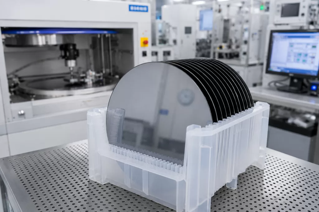
Why SiC Wafer Manufacturing Is Rapidly Evolving
Global electrification has accelerated the adoption of SiC power devices.
Major growth drivers include:
- Electric vehicles
- Fast-charging infrastructure
- Renewable energy inverters
- Energy storage systems
- Industrial automation
- Smart grids
- High-speed rail
- Aerospace power systems
- Data centers
- AI power supplies
Compared with silicon devices, SiC MOSFETs and Schottky diodes enable:
- Higher switching frequencies
- Lower switching losses
- Smaller passive components
- Higher operating temperatures
- Increased power density
- Improved system efficiency
As demand grows, wafer manufacturers must simultaneously improve production capacity and wafer quality.
The future of SiC manufacturing is therefore centered on three key objectives:
- Larger wafer diameters
- Lower crystal defect density
- Higher production yield
Trend 1: Transition from 150 mm to 200 mm SiC Wafers
One of the most significant developments is the industry’s transition from 150 mm (6-inch) to 200 mm (8-inch) SiC wafers.
For many years, 100 mm and 150 mm wafers dominated commercial production. However, leading semiconductor manufacturers are now investing heavily in 200 mm production lines.
Why Larger Wafers Matter
Increasing wafer diameter significantly improves manufacturing efficiency.
Advantages include:
- More chips per wafer
- Lower cost per device
- Better equipment utilization
- Higher throughput
- Improved factory productivity
- Lower manufacturing cost
For example, a 200 mm wafer provides substantially more usable area than a 150 mm wafer, allowing manufacturers to produce significantly more devices during each processing cycle.
This directly reduces the cost of ownership for automotive and industrial power devices.
Challenges of Manufacturing 200 mm SiC Wafers
Producing larger wafers is far more difficult than simply increasing crystal size.
Manufacturers must overcome challenges such as:
- Crystal growth stability
- Thermal stress
- Crystal cracking
- Wafer bow
- Warp control
- Thickness uniformity
- Flatness control
- Surface polishing
- Equipment compatibility
- Defect distribution
Maintaining uniform crystal quality across an 8-inch boule requires much tighter process control than smaller wafers.
Trend 2: Continuous Reduction of Crystal Defects
Defect density remains one of the biggest factors limiting SiC device performance and manufacturing yield.
Unlike silicon, SiC crystal growth is considerably more complex.
Common crystal defects include:
- Micropipes
- Basal plane dislocations (BPD)
- Threading screw dislocations (TSD)
- Threading edge dislocations (TED)
- Stacking faults
- Triangular defects
- Carrot defects
- Polytype inclusions
- Grain boundaries
- Surface pits
Each defect type can negatively affect device reliability.
For example:
- Micropipes can cause device failure.
- Basal plane dislocations may degrade bipolar device performance.
- Surface defects increase epitaxial process risks.
- Stacking faults reduce long-term reliability.
Future manufacturing aims to minimize every major defect category through improved crystal growth and wafer processing.
Trend 3: Improved Crystal Growth Technology
The quality of every SiC wafer begins with crystal growth.
Most commercial SiC boules are produced using Physical Vapor Transport (PVT).
Future improvements focus on:
- Better temperature control
- Stable thermal gradients
- Improved seed crystal quality
- Reduced contamination
- Optimized crucible design
- Enhanced powder purity
- Longer growth cycles
- Better crystal uniformity
Advanced simulation software is also helping manufacturers optimize thermal fields before actual production begins.
These improvements reduce crystal stress and improve boule consistency.
Trend 4: Better Surface Quality
As semiconductor devices continue to shrink, wafer surface quality becomes increasingly important.
Manufacturers are pursuing:
- Lower surface roughness
- Reduced subsurface damage
- Better edge quality
- Fewer polishing scratches
- Improved flatness
- Lower total thickness variation (TTV)
- Better bow control
- Improved warp control
High-quality polishing directly influences:
- Epitaxial growth
- Photolithography
- Device yield
- Process repeatability
Future polishing technologies will combine:
- Precision grinding
- Chemical mechanical polishing (CMP)
- Automated inspection
- AI-assisted process control
Trend 5: Advanced Defect Inspection Technologies
Inspection technology is evolving rapidly.
Modern SiC wafer production increasingly relies on automated optical inspection systems capable of detecting extremely small defects.
Future inspection methods include:
- AI-based image recognition
- High-resolution optical microscopy
- Laser scattering inspection
- Photoluminescence mapping
- X-ray topography
- Raman spectroscopy
- Surface defect mapping
- Crystal defect classification
Rather than simply identifying defective wafers, future systems will predict potential process failures before they occur.
Trend 6: Artificial Intelligence in Manufacturing
Artificial intelligence is beginning to transform semiconductor manufacturing.
Future SiC wafer factories will use AI to optimize:
- Crystal growth parameters
- Grinding conditions
- Polishing recipes
- Equipment maintenance
- Process monitoring
- Yield prediction
- Defect classification
- Predictive maintenance
- Production scheduling
Instead of relying solely on operator experience, AI algorithms can analyze thousands of process variables simultaneously to identify subtle trends that affect wafer quality.
This enables faster process optimization and improved manufacturing consistency.
Trend 7: Smart Manufacturing and Digital Factories
Industry 4.0 technologies are becoming standard in advanced semiconductor manufacturing.
Future SiC production lines will feature:
- Fully automated material handling
- Robotic wafer transport
- Real-time process monitoring
- Equipment connectivity
- Digital twins
- Cloud-based production analysis
- Automatic recipe optimization
- Statistical process control (SPC)
These systems reduce human error while improving productivity and traceability.
Trend 8: Higher Epitaxial Wafer Quality
The substrate and epitaxial layer must work together to achieve high-performance power devices.
Future improvements include:
- Better substrate surface quality
- Improved off-axis angle control
- More uniform epitaxial thickness
- Lower background doping
- Reduced defect propagation
- Better interface quality
Higher-quality substrates produce higher-quality epitaxial wafers, resulting in better device reliability.
Trend 9: Improved Yield Throughout the Manufacturing Process
Manufacturing yield affects profitability as much as wafer quality.
Yield improvements will come from:
- Better incoming crystal inspection
- Automated wafer mapping
- Reduced handling damage
- Improved edge grinding
- Lower contamination
- Optimized polishing
- Better process monitoring
- Equipment automation
- AI-assisted defect prediction
Even small yield improvements can significantly reduce manufacturing costs when thousands of wafers are processed each month.
Trend 10: Greater Process Automation
Automation reduces variability introduced by manual operations.
Future factories will automate:
- Wafer loading
- Orientation
- Thickness measurement
- Surface inspection
- Grinding
- Polishing
- Cleaning
- Packaging
- Traceability
- Final inspection
Automation also improves consistency between production batches.
Trend 11: Sustainable Manufacturing
Environmental sustainability is becoming increasingly important.
Manufacturers are working to reduce:
- Energy consumption
- Water usage
- Chemical waste
- Slurry consumption
- Scrap rates
- Carbon emissions
Future factories will increasingly recycle:
- Grinding coolant
- Process water
- Polishing slurry
- Heat energy
- Manufacturing waste
These initiatives reduce both environmental impact and operating costs.
Trend 12: Supply Chain Localization
To improve supply chain resilience, many regions are investing in domestic SiC production.
Future growth is expected in:
- North America
- Europe
- China
- Japan
- South Korea
This regional expansion helps shorten lead times, improve supply security and support local semiconductor ecosystems.
Trend 13: Better Integration with Advanced Packaging
As power modules become more compact, SiC wafers must support increasingly sophisticated packaging technologies.
Future manufacturing will place greater emphasis on:
- Better wafer flatness
- Improved edge integrity
- Reduced particle contamination
- High-quality backside processing
- Stable wafer thickness
- Better compatibility with wafer bonding
- Improved thermal management
These improvements are essential for advanced packaging processes such as direct copper bonding, wafer-level packaging and heterogeneous integration.
Future Technical Priorities
Over the next decade, SiC wafer manufacturers are expected to focus on several critical performance indicators:
| Manufacturing Target | Future Direction |
|---|---|
| Wafer Diameter | Transition from 150 mm to 200 mm |
| Defect Density | Continuous reduction |
| Crystal Quality | Improved boule uniformity |
| Surface Roughness | Lower Ra values |
| Flatness | Better TTV, Bow and Warp control |
| Yield | Higher overall manufacturing yield |
| Automation | Fully automated production lines |
| Inspection | AI-assisted defect detection |
| Sustainability | Lower energy and water consumption |
| Cost | Reduced cost per device |
What Buyers Should Look for in Future SiC Wafer Suppliers
As manufacturing technologies evolve, buyers should evaluate suppliers based on more than current specifications.
Important considerations include:
- Capability to supply 200 mm wafers
- Stable crystal growth technology
- Low defect density
- Advanced inspection systems
- Process traceability
- Consistent wafer mapping
- Tight flatness control
- Reliable polishing quality
- Strong quality management system
- Long-term production capacity
Suppliers investing in next-generation manufacturing technologies are better positioned to support future semiconductor applications.
Conclusion
The future of SiC wafer manufacturing is driven by the industry’s pursuit of larger wafer diameters, lower defect densities and higher production yields.
Advances in crystal growth, precision machining, AI-assisted inspection, smart manufacturing and automation are enabling manufacturers to produce wafers with greater consistency and lower cost than ever before.
As 200 mm SiC wafers become increasingly commercialized and defect control technologies continue to improve, SiC will play an even more significant role in electric vehicles, renewable energy systems, industrial automation and next-generation power electronics.
For buyers, selecting suppliers with advanced manufacturing capabilities, robust quality-control systems and long-term technology roadmaps will be essential to ensuring reliable device performance and sustainable production growth.
Frequently Asked Questions
Why is the industry moving toward 200 mm SiC wafers?
Larger wafers produce more chips per wafer, improving equipment utilization and reducing manufacturing costs.
What is the biggest challenge in SiC wafer manufacturing?
Maintaining low crystal defect density while producing larger-diameter boules remains one of the most difficult challenges.
How does AI improve SiC wafer production?
AI can optimize process parameters, detect defects, predict equipment maintenance needs and improve overall manufacturing yield.
Why is defect density so important?
Crystal defects can reduce device performance, lower yield and shorten the lifetime of power semiconductor devices.
Will SiC replace silicon completely?
No. Silicon will continue to dominate many low- and medium-power applications, while SiC is expected to expand rapidly in high-voltage, high-power and high-efficiency systems where its material advantages provide significant performance benefits.