
Basal Plane Dislocations in 4H-SiC: Why a Small Crystal Defect Can Become a Long-Term Reliability Problem
Not all defects in a silicon carbide wafer have the same impact. Some imperfections may primarily affect surface appearance. Others can reduce device yield immediately. A particularly important class of defects is more difficult to manage because the device may initially appear normal but degrade during operation. One of the best-known examples in 4H-SiC is […]
SiC Wafer Polishing in 2026: Why Subsurface Damage Matters as Much as Surface Roughness
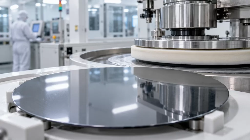
Silicon carbide is one of the most attractive semiconductor materials for high-voltage and high-power electronics, but it is also one of the most difficult wafer materials to process. Its high hardness, strong chemical stability and excellent wear resistance are major advantages in demanding device applications. During wafer manufacturing, however, the same properties make grinding and […]
SiC Wafer Market in 2026: Why Price Is Giving Way to Yield, Quality and 200 mm Qualification
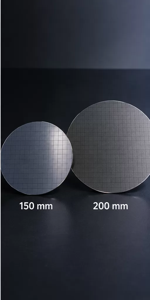
For much of the recent silicon carbide cycle, the discussion around SiC wafers was dominated by two subjects: capacity and price. Suppliers added crystal-growth capacity, Chinese manufacturers expanded aggressively, 150 mm substrate prices declined, and almost every major SiC producer announced a roadmap toward 200 mm production. In 2026, however, the market is entering a […]
SiC Epi-Wafer Uniformity for High-Temperature Electronics: Epitaxy Thickness, Doping, Defects and 6-Inch Wafer-Level Qualification
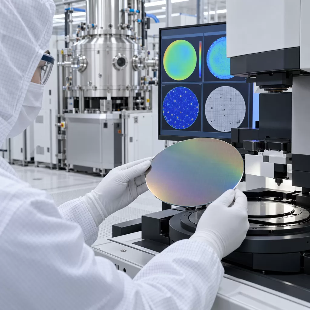
Silicon carbide is increasingly being considered for electronic systems that must operate beyond the practical temperature limits of conventional silicon electronics. Applications such as aerospace sensing, jet engines, geothermal drilling, industrial furnaces and extreme-environment monitoring require semiconductor devices that can maintain stable electrical characteristics under severe thermal conditions. For these applications, however, high-temperature performance cannot […]
Laser Stealth Dicing of SiC Wafers: Subsurface Microcracks, Edge Chipping, Dicing Quality, Inspection and Yield Control
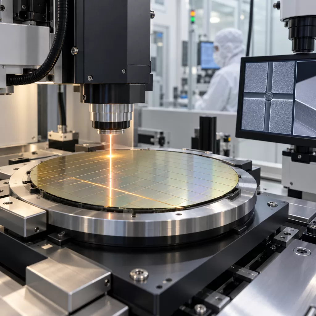
Silicon carbide wafers are increasingly used in high-power and high-temperature semiconductor devices, but they also present major challenges during singulation. Because SiC is extremely hard and brittle, conventional blade dicing can cause edge chipping, kerf loss, mechanical stress and tool wear. As device structures become smaller and wafer value increases, manufacturers are paying more attention […]
Thin SiC Wafer Handling from Backgrinding to Dicing: Ring Frame Mounting, Tape Stress, Warpage and Edge Chipping Control
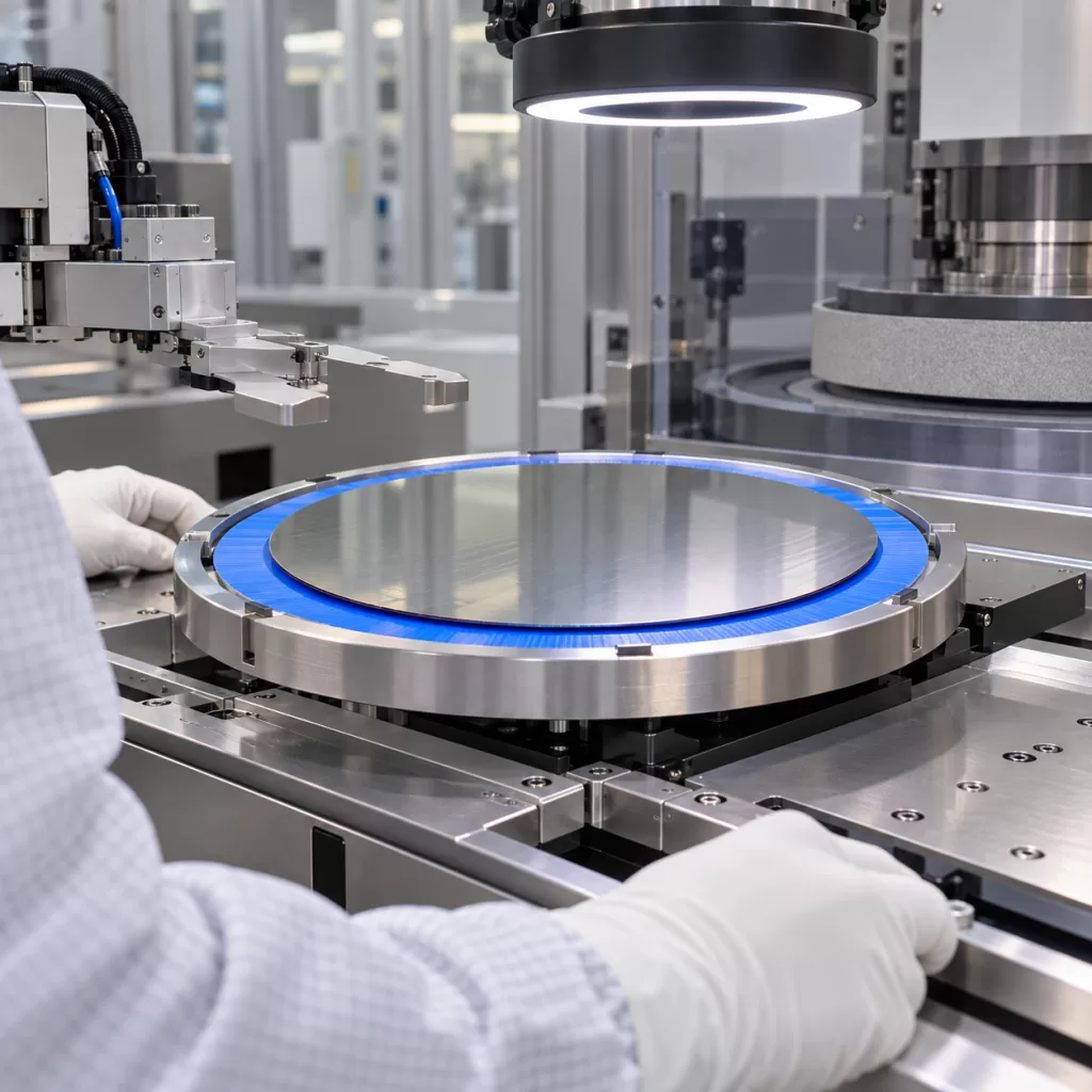
As silicon carbide wafers move toward thinner substrates for power semiconductor manufacturing, wafer handling becomes increasingly important. A standard SiC wafer may remain relatively rigid during conventional processing, but after backgrinding, the reduction in thickness significantly increases sensitivity to bending stress, local pressure, tape tension and mechanical impact. For thin SiC wafers, the transition from […]
GaN Wafer Supply Chain in 2026: Gallium Availability, Substrate Choice, Epitaxy Capacity, Lead Time
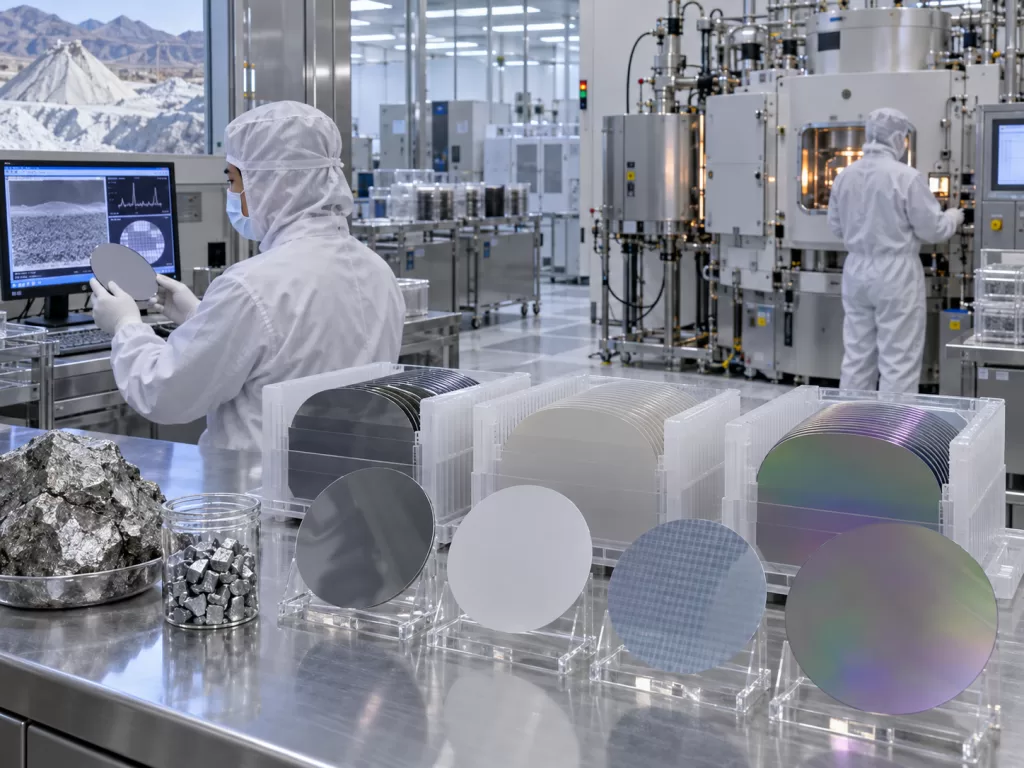
The GaN wafer supply chain in 2026 is no longer determined only by epitaxial performance. Material availability, gallium supply, substrate diameter, epitaxy capacity, export compliance, wafer qualification and manufacturing lead time have all become important factors when RF and power semiconductor manufacturers select a GaN wafer supplier. At the same time, the term “GaN wafer” […]
SiC Wafers for 800VDC AI Data Centers: Substrate Resistivity, Epitaxy, Defect Density and Reliability Requirements
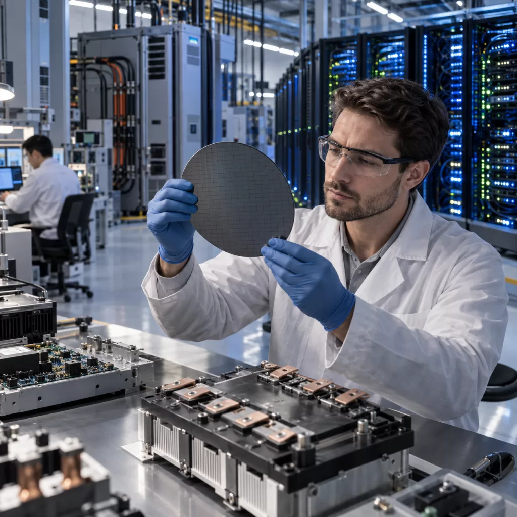
AI data centers are rapidly moving toward higher rack power, higher power density and more efficient electrical distribution. One of the most important changes is the emergence of 800 VDC power architectures. NVIDIA is developing 800 VDC infrastructure for next-generation AI factories as traditional low-voltage rack distribution becomes increasingly difficult to scale to hundreds of […]